


Hard Drive Printed Circuit Board Design and Manufacturing Explained
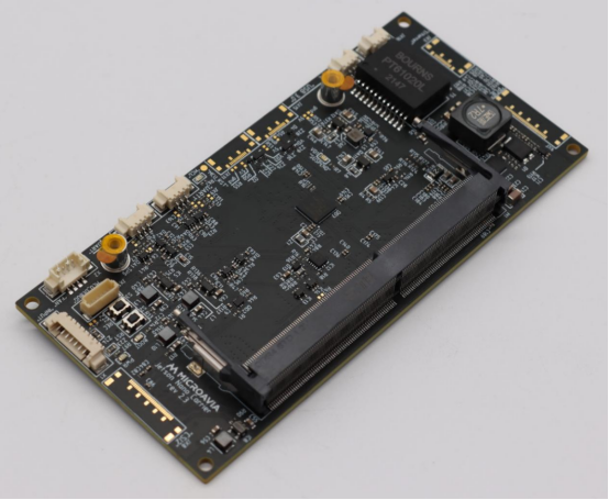
A hard drive printed circuit board (HDD PCB) is the control center of a hard disk drive. It connects the drive’s mechanical parts—the spinning platters, actuator, and read/write heads—to the computer, directing every movement and data exchange.
Often called the brain of the hard drive, the PCB manages power delivery, signal conversion, and data control. It ensures that each bit of information is read, written, and transferred with precision.
Because every operation depends on these electronic pathways, the design and manufacturing quality of the PCB directly determine how reliably a hard drive performs. A well-engineered board maintains signal integrity, resists heat and vibration, and safeguards data accuracy—while even minor design flaws can cause instability or data loss.
In essence, the hard drive’s performance, speed, and durability all begin with one foundation—the printed circuit board that brings its electronic intelligence to life.
Inside the Hard Drive PCB: Functions and Components
Core Functions
The hard drive printed circuit board (HDD PCB) serves as the electronic command center that synchronizes every part of the drive. It regulates power distribution and data communication between the spinning platters, read/write heads, and the computer’s interface. Each electrical signal sent through the PCB determines how data is stored, accessed, and transferred.
One of its key roles is to control the spindle motor and actuator. The spindle motor keeps the platters rotating at a constant speed—often 5,400 or 7,200 RPM—while the actuator positions the read/write heads precisely above each data track. Even slight timing errors can cause data corruption, so the PCB continuously monitors and adjusts these movements.
Another vital function is managing firmware operations and cache buffering. The firmware stored on the PCB’s microcontroller directs how the drive interprets commands from the operating system. Temporary cache memory, often DRAM or NAND, holds frequently accessed data, helping the drive respond faster and reducing latency during read/write operations.
In essence, the HDD PCB coordinates mechanical precision with electronic intelligence—ensuring smooth, reliable communication between the hard drive’s moving parts and the digital world.
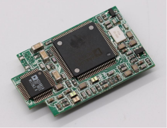
Main Components and Their Roles
A modern HDD PCB integrates several specialized components, each designed for a specific control task. Together, they transform raw electrical input into organized data operations.
Controller IC (Microcontroller):
Acts as the brain of the PCB, running the firmware that controls every action of the drive. It manages error correction, command execution, and communication with the computer via SATA or SAS interfaces.
Motor Driver IC:
Powers and regulates the spindle motor and actuator arm. It converts control signals into precise electrical currents that drive mechanical motion. Stable motor control ensures consistent rotation speed and accurate head positioning.
Cache Memory (DRAM or NAND):
Functions as the temporary data buffer between the controller and the storage platters. For example, when large files are accessed, the cache stores segments of data for quick retrieval, significantly improving transfer speed.
Power and Data Connectors:
Provide stable electrical input and data communication channels. These connectors bridge the PCB to the drive’s internal circuits and the host system, ensuring a steady power supply and seamless data flow.
If you visualize an annotated HDD PCB layout, you would see the controller IC near the data interface port, the motor driver close to the spindle connector, and the cache memory positioned nearby for high-speed signal access. Each element is carefully placed to balance performance, heat dissipation, and signal integrity.
Together, these components form a tightly integrated system that allows the hard drive to function with the speed, precision, and reliability that modern data storage demands.
PCB Design Principles for Hard Drives
Design Requirements
Designing a hard drive PCB requires balancing size, performance, and reliability. The layout must be compact to fit within standard 2.5” and 3.5” hard drive form factors. Despite the limited space, the board must maintain high signal integrity and minimize electrical noise, which is crucial for accurate data transfer.
Controlled impedance is essential for SATA and SAS interfaces. This ensures that high-speed signals travel with minimal reflection or distortion, reducing errors during read/write operations.
Thermal and mechanical stability are also critical. PCBs must handle heat generated by ICs and motors while resisting vibration caused by spinning platters. Proper thermal design prevents overheating, and mechanical robustness ensures the board maintains functionality even under shock or vibration.
Material Selection
The choice of PCB materials directly impacts performance and durability. Common base materials include:
FR-4: Cost-effective, standard performance for general-purpose boards.
High-Tg laminates: Provide better heat resistance and dimensional stability.
Polyimide: Used for flexible zones or specialized high-temperature areas.
High-speed or high-frequency drives may use materials like Rogers or IT-180A, which offer lower signal loss and better high-frequency performance. Key criteria when selecting materials include:
Dielectric constant (Dk): Affects signal speed and impedance.
Loss factor (Df): Low values reduce signal attenuation.
Heat resistance: Ensures the PCB maintains shape and performance under thermal stress.
For example, using FR-4 in a high-speed SATA III drive may result in slight signal degradation, while a high-speed laminate maintains cleaner data transmission.
Layer Stack-Up and Routing Strategy
Most hard drive PCBs use a 4–8 layer stack-up, separating signal and power planes. This separation reduces electromagnetic interference (EMI) and improves signal integrity.
Differential pair routing is used for high-speed data lines, ensuring that paired signals travel together to reduce noise and maintain timing.
Ground plane design is essential for shielding sensitive signals and providing a stable reference for voltage levels. Careful placement of power and ground planes helps minimize crosstalk and EMI, which is especially important in compact 2.5” drives.
Thermal and Mechanical Considerations
Heat management starts with component placement. Heat-generating ICs, such as the controller or motor driver, are positioned near thermal vias or copper pours to dissipate heat efficiently.
Thermal vias and large copper areas act as heat sinks, conducting heat away from sensitive components.
Mechanical integrity is maintained by ensuring the PCB is rigid enough to avoid warping during assembly or operation. The board’s thickness, support from the drive chassis, and controlled laminate properties all contribute to preventing warpage, which could otherwise misalign critical connections.
This design approach ensures that the hard drive PCB remains compact, electrically reliable, and thermally stable, supporting consistent performance and long-term durability in both desktop and enterprise storage applications.
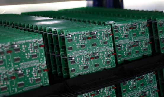
Manufacturing Process of Hard Drive PCBs
Fabrication Steps
The production of a hard drive PCB begins with substrate preparation and copper cladding. The substrate, often FR-4 or high-Tg laminate, provides the mechanical base, while thin copper layers form the conductive pathways.
Next comes imaging and etching, where photoresist masks are applied, and unwanted copper is removed to define circuit patterns. Lamination follows for multilayer boards, bonding inner signal and power layers under heat and pressure. In high-density PCBs, microvias—tiny drilled holes—connect internal layers, enabling complex signal routing within a compact footprint.
After drilling, the board undergoes plating, adding copper to the via walls and surface pads. A solder mask protects traces from oxidation and shorts, while surface finishes like ENIG (Electroless Nickel Immersion Gold) or HASL (Hot Air Solder Leveling) prepare pads for component soldering.
Step-by-step multilayer lamination example:
1. Inner layers are etched and cleaned.
2. Prepreg layers (insulating sheets) are stacked between the inner layers.
3. Heat and pressure bond the layers into a solid board.
4. Final drilling and plating connect the layers electrically.
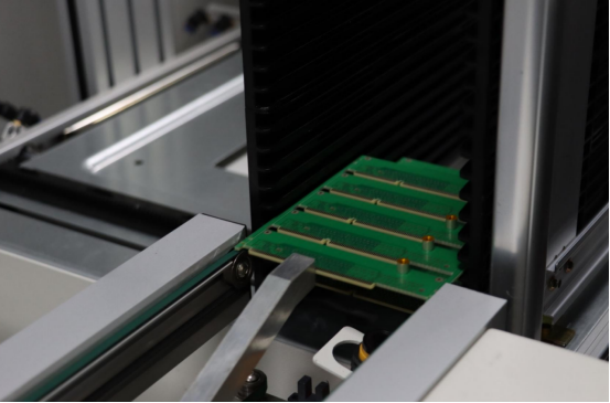
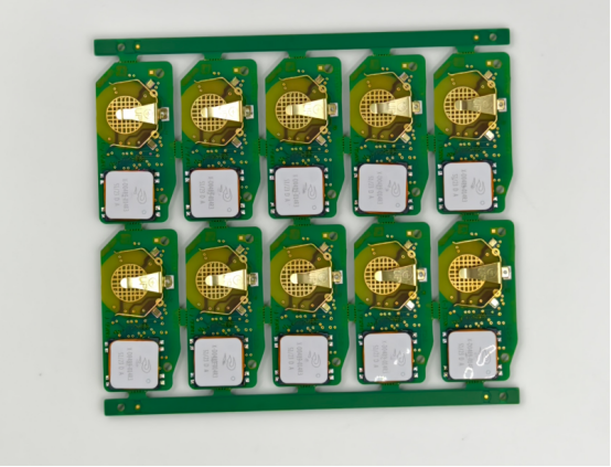
Component Assembly and Soldering
Once fabricated, the PCB moves to component assembly. Surface-mount technology (SMT) places ICs, resistors, capacitors, and other passives precisely on the pads. Automated pick-and-place machines ensure accurate positioning even for tiny components.
Reflow soldering melts solder paste to secure components. Temperature profiles are carefully controlled to avoid damaging sensitive ICs while achieving reliable solder joints.
After soldering, boards undergo rigorous inspection. Automated Optical Inspection (AOI) checks for misplaced or missing parts, In-Circuit Testing (ICT) verifies electrical connectivity, and X-ray systems detect hidden defects like voids in solder joints or internal via issues.
Firmware Loading and Functional Testing
A critical step in HDD PCB manufacturing is firmware installation. The controller IC receives drive-specific firmware and adaptive calibration data, which fine-tunes the read/write behavior for each hard drive.
Following installation, the PCB undergoes functional testing, including:
Power-on diagnostics to confirm basic operation.
Signal verification ensuring proper communication with SATA/SAS interfaces.
Read/write tests using simulated data transfers to validate speed and accuracy.
Automation plays a key role in testing consistency. Robotic handlers and automated test benches allow thousands of boards to be tested with minimal human error, ensuring every HDD PCB meets strict quality and performance standards.
This structured manufacturing process—from substrate preparation to firmware validation—ensures that each hard drive PCB is precise, reliable, and ready to support high-speed, long-lasting storage operations.
Quality Control and Reliability Assurance
Electrical and Functional Testing
Ensuring a hard drive PCB works reliably starts with electrical and functional testing. Impedance testing measures the resistance to signal flow along high-speed traces, verifying that the board maintains proper signal integrity for SATA or SAS data lines. Deviations in impedance can cause data errors or slow transfer speeds.
Power distribution is also checked to confirm that voltage levels reach all critical components without drop or fluctuation. Short-circuit tests identify unintended connections that could damage ICs or other circuitry.
To ensure internal connections are sound, manufacturers perform cross-section analysis of vias. By inspecting microvias under a microscope, engineers can detect voids, misalignment, or insufficient plating, which could compromise signal paths and long-term reliability.
Environmental Stress Testing
Hard drive PCBs must withstand real-world operating conditions. Thermal cycling subjects the board to repeated temperature changes to simulate startup and heavy-use conditions. Vibration testing mimics the mechanical stresses caused by spinning platters, and humidity testing checks resistance to moisture that could lead to corrosion or short circuits.
These tests follow international standards such as IPC-6012 (performance and construction of rigid PCBs) and IEC-60068 (environmental testing for electronics). Compliance ensures consistent performance under stress and helps predict long-term durability.
For context, HDD PCBs are generally subjected to stricter environmental testing than consumer electronics PCBs. While a smartphone PCB might tolerate occasional heat and vibration, an HDD PCB is engineered for continuous operation with high rotational speeds, making thermal and mechanical reliability essential for data integrity.
Through meticulous electrical validation and rigorous environmental stress testing, manufacturers ensure that each hard drive PCB is capable of delivering stable, long-term performance, safeguarding both the drive’s mechanical components and the data stored within.
Common Failures and Repair Practices
Typical Failure Modes
Hard drive PCBs can fail in several ways, often affecting data access or rendering the drive completely inoperative. Burnt traces, shorted components, or motor driver failures are common issues caused by overheating, power surges, or manufacturing defects. These failures can prevent the spindle motor from spinning or the actuator from moving correctly.
Another frequent problem is EEPROM or firmware chip corruption. The firmware stored on the PCB contains essential instructions for reading, writing, and calibrating the drive. Corruption can result from improper firmware updates, power interruptions, or static discharge, leading to unrecognized drives or read/write errors.
Overvoltage or static damage can also occur, particularly if the drive is exposed to electrical surges or mishandled during installation. Even minor electrostatic discharge (ESD) events can damage sensitive ICs, causing partial or complete PCB failure.
Diagnosing and Replacing a Hard Drive PCB
Diagnosing PCB issues begins with visual inspection and multimeter testing. Burn marks, damaged traces, or blown capacitors are often visible under magnification. Voltage checks with a multimeter can identify faulty power distribution or shorted components.
When replacement is necessary, finding a compatible donor PCB is critical. The donor must match the original drive’s model, PCB revision, and firmware version. Using mismatched firmware can prevent the drive from functioning or risk data loss.
A typical step-by-step PCB replacement for data recovery includes:
1. Remove the hard drive from the computer or enclosure.
2. Carefully disconnect the old PCB from the drive, noting connector orientation.
3. Mount the donor PCB, ensuring it matches the firmware revision.
4. Transfer the original EEPROM or ROM chip if necessary to preserve calibration data.
5. Reassemble the drive and run a power-on and read/write test to verify operation.
By following these diagnostic and replacement practices, technicians can often restore drive functionality and recover critical data without compromising the mechanical or magnetic integrity of the hard drive.
Future Trends in Hard Drive PCB Technology
Miniaturization and Integration
Hard drive PCBs are increasingly embracing miniaturization and integration. Modern designs use System-on-Chip (SoC) solutions, combining multiple functions—such as motor control, data processing, and error correction—into a single chip. This reduces board complexity, saves space, and improves energy efficiency.
In addition, compact PCBs are being developed for hybrid HDD-SSD architectures. These designs integrate traditional spinning platters with NAND flash memory on the same board, requiring dense layouts and precise routing to maintain high-speed performance while keeping the drive’s form factor small.
Advanced Manufacturing Innovations
Manufacturing technology for HDD PCBs continues to evolve. High Density Interconnect (HDI) boards with laser-drilled microvias allow for more connections within a smaller area, enabling higher signal density and improved performance.
Another trend is the use of embedded passive components, such as resistors and capacitors, directly within the PCB layers. This reduces component count on the surface and shortens signal paths.
AI-powered inspection systems are also becoming standard in production lines. Automated Optical Inspection (AOI) and X-ray imaging combined with AI algorithms can detect microscopic defects or misaligned components, ensuring higher reliability and lower failure rates.
Sustainability and Recycling
Environmental considerations are shaping the future of HDD PCB production. There is a strong shift toward halogen-free and RoHS-compliant materials, reducing toxic emissions during manufacturing and disposal.
Recycling HDD PCBs presents challenges because they contain complex mixtures of metals and epoxy resins. Recovering valuable metals such as copper, gold, and palladium requires specialized processes, and separating them from non-metallic components remains a key focus for sustainable electronics initiatives.
These trends—miniaturization, advanced manufacturing, and sustainable practices—are driving HDD PCB technology toward smaller, smarter, and more environmentally responsible designs, ensuring that future hard drives continue to deliver high performance while meeting evolving industry and regulatory standards.
Conclusion
The performance and reliability of hard drives rely heavily on precise PCB design and manufacturing. Every detail—from material selection and layer stack-up to signal routing and component placement—affects how efficiently the drive manages data, power, and mechanical motion. A well-engineered PCB ensures stable operation, accurate read/write performance, and long-term durability.
As hard drive technology evolves, PCBs are becoming smaller, more integrated, and environmentally responsible. Trends like SoC integration, high-density interconnects, and halogen-free materials are driving higher data density, improved efficiency, and sustainable production.
For engineers and storage specialists, prioritizing PCB quality is essential. Careful design, rigorous testing, and precise manufacturing practices directly influence drive performance and data security.
If you have questions or want to learn more about PCBs, PCBMASTER is ready to provide expert guidance. As a seasoned PCB supplier, we offer professional solutions and technical support for all your PCB design and manufacturing needs.
FAQs
What is the function of a printed circuit board in a hard drive?
A hard drive printed circuit board (HDD PCB) serves as the drive’s electronic “brain.” It manages power distribution, signal processing, and control logic. The PCB connects the spinning platters, read/write heads, and actuator to the computer, ensuring that data is read, written, and transferred accurately. It also manages firmware operations and temporary cache memory, coordinating mechanical motion with electronic control.
Can a damaged hard drive PCB be repaired or replaced?
Yes, a damaged PCB can often be repaired or replaced, depending on the type of failure. Minor issues, such as burnt traces or faulty capacitors, can sometimes be repaired. In more severe cases, technicians replace the PCB with a compatible donor board, making sure the firmware and EEPROM data match the original drive. Proper replacement allows the drive to function normally and can recover critical data.
What materials are commonly used in hard drive PCBs?
Common materials include:
FR-4: Standard, cost-effective laminate used in most PCBs.
High-Tg laminates: Provide better thermal stability for high-performance drives.
Polyimide: Used in flexible areas or high-temperature zones.
For high-speed or high-frequency applications, materials like Rogers or IT-180A may be used, offering low signal loss and improved data integrity. Material choice affects signal integrity, heat resistance, and overall reliability.
How does PCB design affect data transfer speed and reliability?
PCB design impacts signal integrity, power delivery, and timing accuracy. Features such as controlled impedance traces, differential pair routing, and proper grounding reduce electrical noise and crosstalk. Efficient component placement and thermal management prevent overheating and mechanical stress. Poor design can cause data errors, slow transfer speeds, or drive failure, while precise PCB design ensures fast, stable, and reliable operation.
What are the latest innovations in hard drive PCB manufacturing?
Recent innovations include:
SoC integration: Combining multiple functions on a single chip for compact, efficient designs.
High-Density Interconnect (HDI) and laser-drilled microvias: Allow more connections in smaller boards for higher performance.
Embedded passive components: Reduce surface component count and shorten signal paths.
AI-based inspection: Automated optical and X-ray inspection systems detect microscopic defects, improving reliability.
Sustainable materials: Halogen-free and RoHS-compliant laminates reduce environmental impact.

