


The Complete Guide to Rigid-Flex PCB Design: Materials, Processes, and Key Considerations
As electronic devices continue to evolve towards being lighter, thinner, and more integrated, Rigid-Flex Printed Circuit Boards (PCBs) are becoming an essential technology. Combining the benefits of both rigid and flexible circuits, Rigid-Flex PCBs are increasingly used in applications such as wearable devices, automotive electronics, medical equipment, and aerospace. These boards offer unique advantages in terms of space-saving, flexibility, and reliability—critical features for modern electronics.
The growing demand for advanced, compact electronics is reflected in the rapid expansion of the flexible printed circuit boards market, which was valued at USD 23.89 billion in 2024 and is expected to reach USD 50.90 billion by 2030, growing at a CAGR of 13.7%. This growth is driven by the need for more integrated, high-performance designs, which Rigid-Flex PCBs address perfectly.
In this article, we will explore the design and manufacturing processes of Rigid-Flex PCBs in detail. From material selection to structural design, manufacturing steps, and performance requirements, we’ll provide a comprehensive guide to help you create reliable, cost-effective, and precise Rigid-Flex PCBs.
By the end of this article, you will have a clearer understanding of how to optimize Rigid-Flex PCB designs for the modern electronics industry, ensuring they meet the growing demands for functionality, durability, and miniaturization.
Overview of Rigid-Flex PCBs
1. Definition and Features of Rigid-Flex PCBs
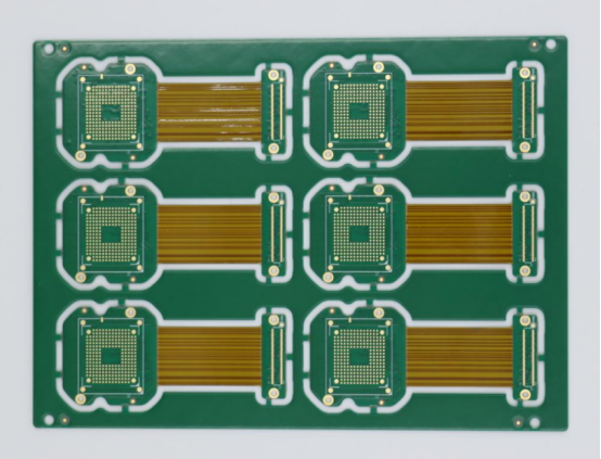
Rigid-Flex PCBs (Rigid-Flexible Printed Circuit Boards) are advanced circuit boards that combine the benefits of both rigid (hard) and flexible PCBs. This unique design merges the mechanical strength of rigid boards with the flexibility of flexible boards, making them an ideal solution for applications where both rigidity and flexibility are required.
The key feature of a rigid-flex PCB is its ability to bend and fold without damaging the circuitry. This is particularly useful in devices with limited space or those that need to be flexible, such as wearables, medical devices, and complex electronics like smartphones or automotive components.
Main Applications:
Miniaturization: Rigid-flex PCBs allow for smaller, lighter devices.
High-Density Circuits: These PCBs can handle high-density circuits in compact spaces.
Bending and Flexing: They can bend without breaking, making them suitable for wearable electronics or gadgets that need to be folded or bent.
Shock and Vibration Resistance: Rigid-flex PCBs are ideal for high-vibration environments, such as automotive and aerospace applications, where flexibility and durability are essential.
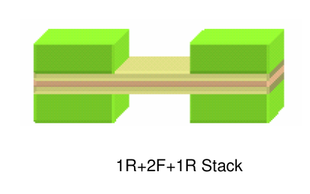
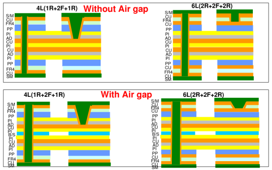
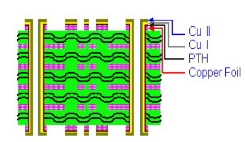
2. Structure of Rigid-Flex PCBs
A rigid-flex PCB consists of two primary parts: the rigid part and the flexible part.
Rigid Part
The rigid part of the PCB is made from traditional materials used in standard rigid PCBs. These materials are typically fiberglass-based and provide structural integrity and mechanical strength. This part of the board remains solid and does not bend. It is often used for mounting components that do not need flexibility and for areas that require durability and protection for the circuits. The rigid sections are often used to mount connectors, ICs, and other fixed components.
Key Features of the Rigid Part:
Provides structural support for the PCB.
Offers durability and stability.
Supports heavy components or those sensitive to movement.
Flexible Part
The flexible part is made from materials such as Polyimide, which is a high-performance plastic known for its excellent flexibility and heat resistance. This part allows the PCB to bend and fold without damaging the circuitry. Flexible PCBs are ideal for applications where the device needs to fit into tight spaces or move, such as in folding smartphones, wearable devices, and flexible displays.
Key Features of the Flexible Part:
Provides flexibility, allowing the PCB to bend or twist.
Typically made from materials like Polyimide or Polyester.
Resistant to heat and mechanical stress, making them durable in harsh conditions.
Design Considerations for Rigid-Flex PCBs
1. Thickness and Material Selection
When designing a rigid-flex PCB, one of the most important factors to consider is the thickness of the board and the materials used. The goal is to minimize the thickness of the PCB while ensuring that it remains durable and functional.
Minimizing Thickness:
Thin boards are essential for applications that require compact designs, such as wearable devices and mobile electronics. Reducing the thickness helps make the product lighter and smaller, which is ideal for consumer electronics.
However, the thickness reduction must be balanced with thermal expansion. When materials with different thermal expansion coefficients are used, they expand and contract at different rates when exposed to heat. This can lead to problems with the adhesion between layers, which may cause the board to fail. Therefore, the thermal expansion difference between the materials, especially between the rigid and flexible parts, should be minimized.
Choosing the Right Materials:
Copper Foil: Copper is the most commonly used conductor material in PCBs. In rigid-flex designs, it is crucial to choose copper foils with the right thickness to ensure proper conductivity and durability, while also taking into account how they interact with other materials.
Polyimide Film: Polyimide is a flexible material that provides excellent heat resistance, making it ideal for the flexible portion of rigid-flex PCBs. It must be compatible with other materials to ensure a strong bond and prevent issues like delamination.
Acrylic Adhesives: Acrylic adhesives are often used to bond different layers of a rigid-flex PCB. Choosing the right adhesive material is critical because it affects the durability of the PCB under stress and temperature fluctuations.
2. Stress Management at Bending Points
Rigid-flex PCBs are often designed to bend or fold in certain areas. However, these bending points can create areas of stress that can damage the PCB over time. Therefore, careful design is needed to manage stress effectively.
Avoiding High-Stress Areas:
When designing a rigid-flex PCB, it’s essential to avoid placing sensitive components or thin traces in areas that will be subjected to bending. High-stress concentrations can lead to cracks, fractures, or failures in the board.
The bending zones should be well-defined and strategically placed to minimize stress. Ideally, bends should be made in areas where there are no critical circuits or components that can be affected by stress.
Dynamic Load and Thermal Impact:
Rigid-flex PCBs need to function under dynamic loads, such as movement or vibration. To ensure mechanical stability, the board must maintain good adhesion between layers and components even during bending.
Thermal shock is another consideration. As the PCB bends, the material properties of different layers can change under temperature variations. The design should ensure that the bending areas remain durable even when exposed to thermal cycling (rapid temperature changes).
3. Flexibility and Shock Resistance
Rigid-flex PCBs are often used in high-shock and vibration environments, such as in automotive electronics or wearable devices. Ensuring flexibility and shock resistance is critical for these applications.
Flexibility:
The flexible part of the rigid-flex PCB must be able to bend without breaking. Materials like Polyimide offer excellent flexibility and can withstand repeated bending without degrading over time.
The design must ensure that the flexible area has enough strength to handle bending cycles, which may occur millions of times in certain applications, such as in wearable electronics like fitness trackers or medical devices.
Shock Resistance:
In environments with high vibration or shock, such as in automotive or military applications, the PCB needs to remain intact despite sudden impacts. The rigid part of the PCB provides the structural support, while the flexible part allows for some movement, helping the PCB withstand shocks without breaking.
Ensuring durability in shock-resistant designs often involves using thicker copper foils and ensuring that the components are securely soldered and spaced to prevent damage during high vibrations.
4. Simplifying the Manufacturing Process
In PCB design, it's essential to consider the manufacturing process to ensure that the board can be produced efficiently and at a low cost. Complex designs can lead to difficulties during production, which can increase costs and decrease the overall quality of the PCB.
Reducing Complexity:
When designing rigid-flex PCBs, the goal is to create a design that is as simple as possible while meeting performance requirements. Complicated designs may lead to difficulties during fabrication, such as difficulty in maintaining precise layer alignment or problems with bonding materials.
A simpler design reduces the chance of defects and improves the yield rate, meaning more good-quality PCBs can be produced from each batch.
Cost Reduction and Improved Yield:
By considering manufacturing limitations, designers can reduce the risk of production errors and avoid using expensive or hard-to-manufacture materials.
Additionally, simplifying the design can help reduce material waste, which directly impacts the cost of production. This is especially important for industries that rely on high-volume manufacturing, such as consumer electronics.
Key Materials for Rigid-Flex PCBs
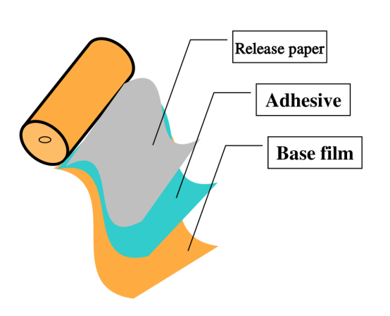
1. Cover Lay (Protective Film)
The Cover Lay is a critical material used in rigid-flex PCBs. It serves multiple essential functions and is key to ensuring the durability and performance of the PCB.
Function:
The Cover Lay primarily acts as a protective layer over the PCB's circuit traces. It ensures insulation between the circuit and the external environment, helping to prevent electrical short circuits. Additionally, it increases the durability of the PCB by offering protection against physical wear and environmental factors like moisture and chemicals.
Material Properties:
Several types of resins are used in Cover Lay materials, each with different characteristics:
Epoxy Resin: Known for good adhesion and chemical resistance, epoxy resin is widely used in PCBs for its durability and versatility.
Phenolic Resin: Typically offers long storage life and is often used for low-flow applications where resin overflow must be minimized.
Acrylic Resin: Known for its excellent flexibility and easy processing, acrylic resin is suitable for applications that require fast production times.
The main performance requirements for Cover Lay materials include:
Gas Resistance: The material must be able to withstand exposure to gases in harsh environments.
Workability: The material should be easy to process during manufacturing without significant issues.
Flexibility: The material must be flexible to accommodate the bending required for rigid-flex PCBs.
Bend Resistance: The Cover Lay must also maintain its integrity over time when subjected to repeated bending cycles.
Application Specifications:
Film Type: These are typically used for high-precision applications, with thicknesses ranging from 30 µm to 160 µm. This variation in thickness makes them suitable for various types of circuit designs, from simple to complex.
Photo-sensitive Dry Film Type: This type is applied in dry film processes and has a thickness range of 25 µm to 50 µm, ideal for applications requiring microhole processing.
Baking Temperature:
The temperature and baking time for Cover Lay materials can vary depending on the resin type. Typically, the material is baked between 140°C and 165°C to achieve optimal bonding and curing. The baking process helps solidify the resin and ensure it forms a strong, stable protective layer.
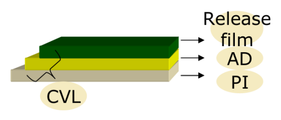
2. Softboard Materials
Softboard materials are an essential component in rigid-flex PCBs, providing the flexible portion of the board. The most commonly used materials include rolled annealed copper foil (RAR copper) and electrolytic copper foil (ED copper).
RAR Copper (Rolled Annealed Copper Foil):
Flexibility: RAR copper is known for its excellent flexibility, making it ideal for fine lines and high-density interconnections in the flexible sections of a rigid-flex PCB.
Smooth Surface: This material provides a smooth surface, which is especially beneficial for high-frequency and high-speed signal transmission, as it reduces signal loss and enhances electrical performance.
Applications: RAR copper is often used in high-end applications such as mobile devices, wearable electronics, and advanced consumer gadgets, where precise, flexible designs are required.
ED Copper (Electrolytic Copper Foil):
Lower Cost: ED copper is more affordable compared to RAR copper, making it suitable for general-purpose PCBs.
Rough Surface: The surface of ED copper is relatively rougher than RAR copper, which can cause higher resistance in high-frequency applications. However, it works well in less demanding environments.
Applications: ED copper is commonly used in rigid PCBs and applications that do not require high-frequency performance or flexible designs.
These copper foils provide the conductive layers for both rigid and flexible sections of the PCB, ensuring efficient signal transmission while accommodating the unique mechanical properties of rigid-flex designs.
Manufacturing Process of Rigid-Flex PCBs
The manufacturing process of rigid-flex PCBs involves several key steps to ensure that the board is durable, functional, and meets the required performance standards. Here's a detailed breakdown of each stage of the process.
1. Pre-Treatment
The pre-treatment process is crucial to prepare the copper surface for bonding and further processing.
Removing Oil and Oxide Layers:
Before any other steps, it's essential to clean the copper surface. This is done by micro-etching, degreasing, and acid cleaning. Micro-etching uses a chemical solution to roughen the copper surface, which helps improve adhesion for later processes. Degreasing removes any oils or contaminants from the surface, while acid cleaning helps remove any oxide layers, ensuring that the copper is clean and ready for bonding.
Cleaning and Drying:
After the surface treatment, the PCB is thoroughly washed to remove any remaining chemicals. It is then dried to prevent contamination. Cleanliness is essential to avoid defects in the final product, such as weak bonding or electrical failure.
2. Lamination and Exposure
Once the surface is prepped, the next step involves applying a protective coating and transferring the circuit pattern.
Lamination with UV Photoresist (Dry Film):
UV photoresist, often in the form of dry film, is used to coat the PCB evenly. This layer will serve as a light-sensitive mask during the exposure process. The dry film is applied evenly on top of the copper surface, ensuring that it covers all areas that will later form the circuit pattern.
Exposure:
The UV exposure process uses ultraviolet light to activate the photoresist. When exposed to UV light, the photoresist undergoes a chemical reaction, causing the areas that are exposed to light to become hardened. These areas will remain on the PCB, while the areas that are not exposed can be easily removed in the next step. This process creates the required circuit pattern on the board.
3. Developing and Etching
After exposure, the next steps involve developing the pattern and etching away unwanted copper.
Developing:
During the development process, the areas of photoresist that were not exposed to UV light are washed away, revealing the copper underneath. This step creates the exact circuit design that was originally mapped onto the PCB.
Etching:
After development, chemical etching is used to remove the excess copper, leaving behind only the desired circuit traces. The etching solution dissolves the copper, ensuring that only the needed circuit paths remain on the board. This step is crucial for creating precise, accurate lines and connections on the PCB.
4. Cover Lay Application
The Cover Lay is a protective layer that is applied to the flexible parts of the rigid-flex PCB.
Purpose of Cover Lay:
The Cover Lay is used to protect the copper traces on the flexible parts of the PCB, ensuring that they are insulated and protected from damage. It helps prevent short circuits, contamination, and physical damage to the circuits during handling or operation.
Application:
The Cover Lay is applied over the flexible sections of the PCB, covering the copper traces and ensuring that they remain intact and functional. This layer is typically a thin film that is bonded to the board using heat and pressure. It adds an extra layer of durability, which is particularly important in high-stress environments where flexibility and reliability are essential.
5. Drilling and Copper Plating
The next step is to create vias or holes in the PCB, which are essential for electrical connections between different layers of the board.
Drilling:
High-precision drilling is used to create tiny holes (vias) that connect the different layers of the PCB. The drilling process requires careful control to ensure the holes are accurate and clean, which is critical for maintaining electrical performance.
Copper Plating:
After drilling, the vias are plated with copper to create electrical connections between the layers. This is done through chemical copper plating followed by electroplating, ensuring that the vias are conductive and capable of carrying signals or power between layers of the PCB.
6. Post-Processing and Quality Testing
Once the main manufacturing steps are completed, the PCB goes through several final processes to ensure its quality and performance.
Electroplating and Durability Testing
Electroplating ensures that all areas of the PCB are adequately coated with copper, providing the necessary conductivity for the circuits. After plating, the board undergoes strength testing to ensure that it meets electrical conductivity standards and mechanical strength requirements.
Quality Inspection
The final product is subjected to a series of quality tests. These tests may include:
Pressure testing to ensure that the PCB can withstand normal operating conditions without failure.
Temperature testing to ensure that the PCB can operate in a variety of environments without degradation.
These tests are essential for confirming that the final product meets the customer's design specifications and is suitable for its intended application.
Key Performance Requirements and Challenges of Rigid-Flex PCBs
Rigid-flex PCBs are essential in applications where both flexibility and high performance are required. However, designing and manufacturing these boards comes with specific performance requirements and challenges. Here, we explore the critical performance characteristics and challenges associated with rigid-flex PCBs.
1. Climatic Resistance
Rigid-flex PCBs must be able to withstand environmental conditions such as temperature fluctuations, humidity changes, and exposure to ultraviolet (UV) light.
Temperature and Humidity Resistance:
Rigid-flex PCBs are often exposed to environments with varying temperatures and humidity levels. For instance, in automotive or aerospace applications, temperature changes can range from extremely cold to very hot conditions. The board's materials must be durable enough to maintain their functionality and performance under these environmental stresses.
UV Resistance:
The board's components must also withstand UV exposure, which can degrade materials over time. UV-resistant coatings or protective layers are often applied to prevent UV degradation. Without this resistance, the PCB’s lifespan could be significantly shortened, leading to failure in the field.
Example: In automotive electronics, a rigid-flex PCB might be exposed to extreme temperatures within the engine compartment. It is crucial that the PCB maintains stable operation despite these varying conditions.
2. High-Temperature Performance
Rigid-flex PCBs used in critical industries such as automotive electronics, aerospace, and military applications must be capable of withstanding high temperatures without losing their mechanical and electrical properties.
Thermal Stability:
High-temperature environments, such as in engines or outer space, require materials that can endure prolonged exposure to heat without degrading. The materials used for rigid-flex PCBs, including the copper foil, flexible films, and adhesives, must have high thermal resistance. These materials ensure that the board remains functional and reliable even when exposed to heat up to 200°C or more.
Applications in High-Temperature Environments:
Rigid-flex PCBs are used in environments where high heat is a constant factor. In automotive electronics, for example, rigid-flex PCBs might be used in engine control units or powertrain systems, where high temperatures are common. Similarly, in aerospace, these PCBs need to function in high-temperature regions like engine compartments or satellite systems.
Real-Life Example: A rigid-flex PCB used in a satellite must endure high temperatures during re-entry into the Earth's atmosphere. The PCB material must maintain stability and resist thermal expansion to prevent mechanical failures.
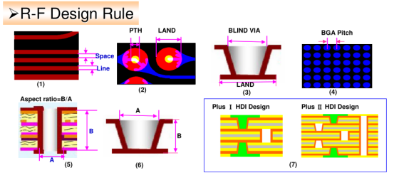
3. Precision and Reliability
Rigid-flex PCBs must meet very precise manufacturing standards, especially when dealing with small apertures and high-density circuits.
Microvia and Fine-Line Precision:
As technology advances, the need for smaller, more compact devices grows. This requires microvias (small holes used to connect different PCB layers) and fine-line circuits. These intricate designs demand extremely precise manufacturing processes. The margin of error is minimal, so the production process must be accurate to prevent circuit failures or poor signal quality.
Reliability:
The reliability of rigid-flex PCBs is paramount. For example, in medical devices or aerospace, where safety is critical, the board must function flawlessly under various conditions, including mechanical stress, temperature extremes, and electrical demands. The reliability is ensured through stringent testing methods, such as thermal cycling, vibration testing, and shock resistance tests.
Real-Life Example: A rigid-flex PCB used in a medical device like a pacemaker must be precisely manufactured to ensure that the small circuits perform reliably over the lifetime of the device, even under the mechanical stress from the human body.
Challenges in Achieving These Requirements
While the performance requirements are clear, achieving them is not always straightforward. Several challenges can arise during the design and manufacturing process.
Material Compatibility:
Combining rigid and flexible materials in one PCB presents challenges. The thermal expansion rates of rigid and flexible materials are often different, which can cause delamination or cracking under thermal stress. Therefore, careful selection of materials with similar expansion rates is essential.
Manufacturing Complexity:
The precision required for high-density designs and microvias means that the manufacturing process must be extremely accurate. This often involves specialized machinery and techniques such as laser drilling, high-precision lamination, and chemical etching. Ensuring tight tolerances while maintaining cost-effectiveness is a constant challenge.
Testing and Validation:
Rigid-flex PCBs are subject to extensive testing before they are deemed reliable for end-use. This can involve thermal, mechanical, and electrical tests to ensure the PCB will function as intended under various real-world conditions. Ensuring consistency in testing across high-volume production is crucial to avoid defects.
Conclusion
As we've explored, rigid-flex PCBs are indispensable in industries requiring high precision, flexibility, and durability. From automotive to aerospace and medical devices, these boards are designed to perform under challenging conditions like extreme temperatures, environmental stress, and high-frequency operations. However, designing and manufacturing these PCBs comes with its own set of challenges, including material compatibility and precision in production.
At PCBMASTER, we understand these challenges and offer solutions that meet your needs. Our 7-day delivery for 10-layer rigid-flex PCBs sets us apart in the industry. Whether you need a standard rigid-flex design or an advanced HDI process, we deliver on time with 6 to 20 layers and use high-quality materials from trusted brands like DuPont, Panasonic, and Shinko. We even offer soft board lengths as small as 0.8mm, perfect for your most intricate designs.
Choose PCBMASTER for fast, reliable, and high-quality rigid-flex PCB manufacturing—we turn your vision into reality, swiftly and efficiently.
FAQs
1. What industries commonly use rigid-flex PCBs, and why?
Rigid-flex PCBs are widely used in industries such as automotive, aerospace, medical devices, consumer electronics, and telecommunications. These industries require high-density, compact, and durable circuits that can withstand extreme conditions like vibration, temperature fluctuations, and space constraints. The flexibility of rigid-flex PCBs allows them to be bent or folded without compromising functionality, making them ideal for applications where size and performance are critical, such as wearable devices, drones, and automotive sensors.
2. What are the benefits of using Polyimide material in rigid-flex PCB design?
Polyimide is a commonly used material in rigid-flex PCBs due to its excellent flexibility, high heat resistance, and chemical stability. Its ability to withstand high temperatures (up to 250°C) makes it ideal for applications in high-temperature environments, such as automotive or aerospace electronics. Additionally, polyimide's durability and ability to bend without cracking allow for designs that can fit in compact, tight spaces while maintaining high reliability. This makes it an essential material in industries where durability and performance under extreme conditions are critical.
3. How does the manufacturing process of rigid-flex PCBs differ from traditional rigid PCBs?
The manufacturing process of rigid-flex PCBs involves additional complexity compared to traditional rigid PCBs. It requires combining both flexible and rigid layers, which involves more precise alignment and bonding processes. Key steps like lamination, drilling, and copper plating are similar but require special techniques to handle the flexible materials without damaging them. In rigid-flex designs, the challenge lies in ensuring the proper integration of these layers while maintaining the mechanical and electrical properties required. The process also includes additional steps such as applying Cover Lay films and precision drilling to create vias for electrical connections, which are not necessary in standard rigid PCBs.

