


Top Techniques for Flexible PCB Fabrication in Modern Electronics
In today’s fast-evolving electronics landscape, devices are getting smaller, lighter, and more versatile than ever. From foldable smartphones to wearable health monitors, the demand for circuits that can bend, twist, and fit into unconventional spaces has skyrocketed. Flexible PCBs have emerged as a critical solution, enabling designers to push the limits of innovation without compromising performance. Understanding the techniques behind their fabrication is essential for anyone looking to create durable, high-performance electronic products that meet the demands of modern applications.
Introduction to Flexible PCB Fabrication
What is Flexible PCB Fabrication?
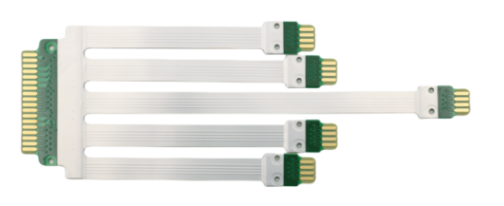
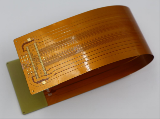
Flexible PCB fabrication refers to the process of designing and manufacturing printed circuit boards that can bend, twist, or fold without losing electrical functionality. Unlike rigid PCBs, which are solid and inflexible, flexible PCBs are made with materials that allow mechanical movement while maintaining stable electrical performance.
The most common substrates used in flexible PCBs are polyimide and PET (polyethylene terephthalate). Polyimide is highly heat-resistant and ideal for high-performance applications, while PET offers a more cost-effective solution for simpler circuits. Copper is typically used as the conductive layer, often in thin, flexible foils that adhere to the substrate.
The key benefits of flexible PCB fabrication include space-saving designs, weight reduction, and enhanced durability. Because these boards can conform to irregular shapes, they are perfect for applications where compactness and light weight are critical. Additionally, their ability to withstand mechanical stress makes them more reliable in dynamic or vibration-prone environments.
Importance in Modern Electronics
Flexible PCBs play a crucial role in modern electronics, enabling the production of smaller, lighter, and more complex devices. They are widely used in smartphones, wearable technology, medical devices, and aerospace applications. For example, the slim, foldable designs of the latest smartphones rely heavily on flexible PCB technology to maintain functionality in compact spaces.
These boards are particularly valuable in high-density and miniaturized circuits, where traditional rigid PCBs would take up too much space or fail under repeated bending. In a practical comparison, a rigid PCB in a smartphone can only support a flat, non-folding structure, limiting design flexibility. In contrast, a flexible PCB allows the same circuitry to wrap around corners or fold inside the device, maximizing space utilization and reducing overall device thickness.
By combining mechanical adaptability with electrical reliability, flexible PCBs have become indispensable in the design of advanced electronic products, setting the foundation for innovations that demand both compactness and high performance.
Core Materials and Design Considerations
Substrate Materials
The substrate material in a flexible PCB is the foundation that provides mechanical support and defines the board’s flexibility. The two most common options are polyimide and PET (polyethylene terephthalate).
Polyimide is highly heat-resistant and can withstand soldering temperatures, making it suitable for high-performance electronics. It also maintains flexibility over repeated bending cycles.
PET is more cost-effective but has lower thermal stability, which limits its use in high-temperature environments. It is ideal for low-power, simple circuits where extreme durability is not critical.
Thickness considerations are crucial for bending and folding. Thinner substrates increase flexibility but may reduce mechanical strength, while thicker substrates provide more support but are less bendable. Designers must balance flexibility, durability, and cost when selecting substrate thickness. For example, a 25 μm polyimide layer can handle tight bends for wearable devices, whereas a 75 μm layer may be better for slightly curved aerospace applications.
Conductive Layers
The conductive layer is usually made of copper foil, and its type significantly affects both flexibility and electrical performance.
Rolled Annealed (RA) copper is softer, highly flexible, and resistant to cracking under repeated bending. It is ideal for dynamic flex circuits.
Electrodeposited (ED) copper is more rigid and cost-effective, making it suitable for static flex applications that do not bend frequently.
Other considerations include current-carrying capacity and signal integrity. Thicker copper supports higher currents but reduces flexibility, while thinner copper is more flexible but may limit the circuit’s power handling. Designers must balance electrical and mechanical requirements, especially in high-density or high-frequency circuits.
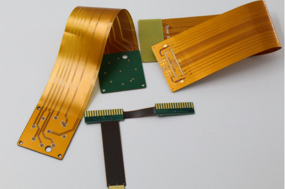
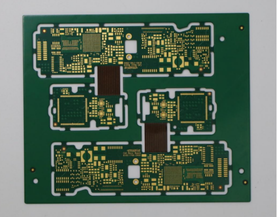
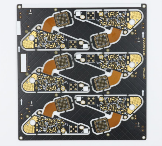
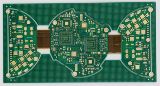
Flexible PCB Stack-Up and Layering
The stack-up of a flexible PCB determines its mechanical reliability and electrical performance. Flexible PCBs can be:
Single-sided – one conductive layer, simplest and most flexible.
Double-sided – two layers connected by vias, suitable for moderate complexity circuits.
Multilayer – three or more layers, enabling high-density routing for advanced electronics.
Planning the stack-up is critical for bending radius and reliability. Designers typically place the outer layers with thinner copper and flexible substrate, while the inner layers may use slightly thicker copper for signal stability.
Step-by-step example of a 4-layer flex PCB stack-up:
1. Layer 1 (Top) – RA copper on polyimide, carrying signal traces.
2. Layer 2 – Polyimide core for insulation and flexibility.
3. Layer 3 – RA copper, carrying power or ground planes.
4. Layer 4 (Bottom) – RA copper on polyimide, for additional signal routing.
This configuration maintains flexibility while supporting complex circuit designs, balancing mechanical durability with electrical performance.
Advanced Fabrication Techniques
Etching Techniques
Etching is the process of removing unwanted copper from a flexible PCB to create the desired circuit pattern. The two main etching methods are wet chemical etching and laser etching.
Wet chemical etching uses acids or chemicals to dissolve copper. It is cost-effective and suitable for mass production but may have limitations in precision for very fine traces.
Laser etching uses focused laser beams to remove copper with high accuracy. It is ideal for high-density and high-precision applications, such as flexible PCBs in wearable electronics.
Example: A high-precision flexible PCB for a medical sensor may use laser etching to create 3–4 mil (0.076–0.102 mm) trace widths that wet etching cannot reliably achieve.
Pros and Cons:
Wet etching: low cost, fast for large volumes, but less precise.
Laser etching: highly precise and customizable, but slower and more expensive.
Flexible PCB Drilling and Via Formation
Vias connect different layers of a flexible PCB. Common types include microvias, through-holes, and blind vias.
Step-by-step via plating process:
1. Drill the via using mechanical or laser methods.
2. Clean the via hole to remove debris.
3. Deposit a thin copper layer inside the via using electroplating.
4. Ensure proper connection between layers by testing conductivity.
Mechanical drilling is cost-effective and suitable for larger holes but can cause substrate stress and debris. Laser drilling produces cleaner, smaller holes with higher precision, reducing the risk of cracking in thin, flexible materials. Choosing the right method depends on via size, quantity, and mechanical flexibility requirements.
Surface Finishes for Flex PCBs
Surface finishes protect copper and improve solderability. Common finishes include:
ENIG (Electroless Nickel Immersion Gold): Provides excellent corrosion resistance and flat surface for fine-pitch components.
HASL (Hot Air Solder Leveling): Cost-effective, but less ideal for thin, flexible circuits due to uneven surfaces.
OSP (Organic Solderability Preservative): Environmentally friendly and provides good solderability for simple designs.
The choice of finish affects reliability and solder performance. For example, ENIG is preferred in high-reliability wearables where multiple soldering cycles may occur.
Bending and Dynamic Flex Testing
Flexible PCBs must withstand repetitive bending and mechanical stress. Dynamic flex testing simulates these conditions in a controlled environment.
Simulation methods: Bending cycles, torsion tests, and thermal cycling.
Key parameters: Minimum bending radius, number of flex cycles, temperature range.
Example: A foldable smartphone uses a flex PCB with a minimum bend radius of 5 mm, tested for over 100,000 folding cycles to ensure durability without trace cracking. Proper testing ensures that flexible PCBs perform reliably in applications such as wearables, foldable devices, and compact aerospace electronics.
Design for Manufacturability (DFM) in Flexible PCBs
Trace and Spacing Guidelines
In flexible PCB design, trace width and spacing are critical for reliability. Minimum trace widths are typically 3–5 mils (0.076–0.127 mm) for standard flex circuits, though advanced processes can achieve finer traces for high-density applications. Minimum spacing depends on voltage requirements and bending stress; designers often maintain at least 3 mils between traces in dynamic flex areas.
Design rules to prevent cracking and stress include:
Avoid routing traces along fold lines; instead, route perpendicular to bending directions.
Use rounded corners in trace patterns to reduce stress concentration.
Limit copper thickness in bendable areas; thinner copper flexes more easily.
These rules help prevent delamination, trace cracking, or signal failure, ensuring long-term durability in devices like wearables and foldable electronics.
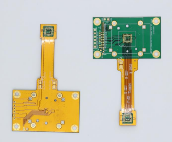
Component Placement Strategies
Proper component placement is essential for mechanical reliability. Components should be located in non-bending areas, leaving flexible zones free to bend without stress.
Example: In a foldable smartphone, rigid ICs and connectors are placed in the non-folding sections of the PCB, while traces and thin flex sections handle the bending. This prevents solder joint fatigue and improves device longevity.
Other strategies include:
Using small, lightweight components in bendable regions.
Avoiding large thermal pads or stiff components in flex zones.
Grouping high-density circuitry in rigid zones to reduce mechanical stress.
Thermal Management and Heat Dissipation
Flexible PCBs often carry heat-sensitive components that require careful thermal management. Without proper design, overheating can damage both the substrate and the circuitry.
Techniques for effective thermal management include:
Copper planes to distribute heat evenly across layers.
Thermal vias to transfer heat from surface components to internal layers.
Heat-spreading materials, such as thin graphite sheets, for uniform dissipation in thin or compact flex circuits.
Example: A wearable health monitor may use thermal vias under a microcontroller to dissipate heat efficiently, preventing hot spots while maintaining the board’s flexibility.
Quality Control and Testing Techniques
Electrical Testing
Electrical testing ensures that a flexible PCB functions correctly before assembly or deployment. The most common methods include continuity testing and isolation testing.
Continuity testing verifies that all intended electrical paths are complete and can carry current.
Isolation testing checks that no unintended connections (short circuits) exist between adjacent traces or layers.
Automated Optical Inspection (AOI) is also widely used for trace integrity. AOI systems scan the PCB with cameras to detect missing traces, misalignments, or defects caused during fabrication. This method is highly efficient for high-volume production and ensures consistent quality.
Mechanical and Environmental Testing
Flexible PCBs are subject to mechanical stress and environmental factors, which can affect reliability over time. Testing includes:
Bend, flex, and torsion tests to simulate repeated folding or twisting in real-world applications.
Thermal cycling to test performance under fluctuating temperatures.
Humidity exposure tests to check for moisture-induced failures in polyimide or PET substrates.
Example: Wearable electronics, such as fitness trackers, undergo dynamic bending tests where the PCB is flexed thousands of times to ensure traces and vias remain intact. Thermal cycling is then applied to simulate body heat and environmental exposure, confirming the board’s long-term durability.
Failure Analysis and Common Defects
Understanding typical defects helps improve the design and fabrication process. Common issues include:
Delamination – separation between substrate layers due to poor adhesion or excessive bending.
Crack formation – fractures in copper traces caused by mechanical stress.
Via failure – incomplete or broken connections between layers, often from improper plating or drilling.
Root-cause analysis approach:
1. Identify the failure location through visual inspection or electrical testing.
2. Analyze the failure type (mechanical, thermal, or fabrication-related).
3. Adjust design rules, material selection, or fabrication processes to prevent recurrence.
This systematic testing and failure analysis ensures that flexible PCBs meet high reliability standards for demanding applications like wearables, aerospace devices, and foldable electronics.
Future Trends in Flexible PCB Fabrication
Emerging Materials
The next generation of flexible PCBs is being driven by innovative substrates and conductive inks. Printed electronics increasingly use thin, flexible polymer substrates combined with silver or carbon-based conductive inks to create circuits that are lightweight, bendable, and suitable for rapid prototyping.
Biocompatible materials are gaining traction for medical wearables. These substrates and inks are non-toxic, skin-friendly, and compatible with long-term contact, enabling flexible PCBs in devices such as continuous glucose monitors, heart rate sensors, and other implantable or wearable medical electronics.
Advanced Manufacturing Technologies
Flexible PCB fabrication is evolving through roll-to-roll processing and additive manufacturing techniques.
Roll-to-roll processing allows continuous fabrication of flexible circuits on a roll of substrate, improving efficiency for high-volume production.
Additive manufacturing (3D printing of conductive inks) enables rapid prototyping of flexible, customized circuit layouts without traditional etching or drilling steps.
Flexible PCBs are also being increasingly integrated with displays and sensors, creating multifunctional devices. For example, foldable smartphones and wearable fitness devices combine flexible PCBs with OLED displays and touch sensors in a single compact module.
Sustainability Considerations
Environmental concerns are shaping the future of flexible PCB fabrication. Eco-friendly materials, such as biodegradable substrates and lead-free soldering, reduce environmental impact. Additionally, recycling strategies for copper, polyimide, and PET waste are being implemented to reclaim valuable materials and reduce landfill contributions.
These sustainable practices not only lower the ecological footprint but also appeal to manufacturers seeking compliance with global environmental regulations, such as RoHS and WEEE.
Conclusion
Modern flexible PCB fabrication combines advanced materials, precise manufacturing techniques, and thoughtful design strategies to create circuits that are reliable, high-performance, and space-efficient. From substrate selection and trace design to bending tests and surface finishes, every step impacts durability and functionality in applications ranging from wearables to foldable smartphones and aerospace electronics.
At PCBMASTER, we deliver cutting-edge solutions, including soft-rigid PCBs with 6–20 layers, fast 7-day turnaround for standard 10-layer boards, and support for HDI first-order to multi-order flex-rigid designs using premium materials from DuPont, Panasonic, and Shenggao. Our processes can achieve flexible sections as thin as 0.8 mm, ensuring maximum adaptability without compromising reliability.
By integrating innovation, quality control, and sustainability, flexible PCBs continue to enable compact, high-performance electronic designs for the next generation of devices.
FAQs
What are the main advantages of flexible PCBs over rigid PCBs?
Flexible PCBs can bend, twist, and fold, allowing electronic designs to fit into compact or irregular spaces. They offer space-saving, weight reduction, and improved durability compared to rigid PCBs. Flexible circuits are ideal for wearables, foldable smartphones, and medical devices where movement or tight integration is required. Additionally, flexible PCBs reduce assembly complexity by connecting multiple components with fewer interconnects.
How do bending radius and material selection affect PCB longevity?
The bending radius is the minimum curve a flexible PCB can handle without damaging traces or causing delamination. A tighter radius increases stress and reduces lifespan. Material selection, such as polyimide versus PET, determines flexibility, thermal tolerance, and mechanical strength. Using heat-resistant and flexible materials like polyimide improves durability under repeated bending, while stiffer or lower-quality materials can fail sooner in dynamic applications.
What are the common challenges in multilayer flexible PCB fabrication?
Multilayer flexible PCBs face several challenges:
Layer alignment and registration, which must remain precise despite substrate flexibility.
Via formation, especially microvias, which require high precision to avoid connection failures.
Stress management, as bending can cause cracks, delamination, or trace failure if copper thickness, substrate choice, or stack-up design is not optimized.
Careful material selection, layer stack planning, and testing are essential to overcome these challenges.
How does laser etching compare to chemical etching in flex PCB production?
Laser etching uses focused beams to remove copper with high precision, making it ideal for fine traces and high-density designs. It produces clean edges and reduces mechanical stress. Chemical (wet) etching is more cost-effective for large-scale production but may struggle with very small traces and intricate patterns. Laser etching is preferred when accuracy and miniaturization are critical, though it is generally slower and more expensive than chemical etching.
Can flexible PCBs be used in high-power electronics?
Yes, flexible PCBs can handle high-power applications, but design considerations are critical. Thicker copper layers and wider traces are needed to carry higher currents without overheating. Thermal management techniques, such as copper planes, thermal vias, and heat-spreading materials, are used to dissipate heat efficiently. With proper material selection and design, flexible PCBs can reliably support power-intensive devices, including industrial electronics and power modules.

