90-Ohm Microstrip on IC Substrates: Real vs. Calculated Impedance
In advanced IC packaging, even a few ohms of impedance drift can be the difference between a clean high-speed channel and a system that quietly fails in the field. Many engineers still rely on PCB-oriented tools like Polar Si9000 to estimate microstrip impedance on packaging substrates, assuming the structures behave the same. They don’t.
Once the substrate enters the molding process, everything changes. The top-layer traces no longer “see” air—they’re surrounded by layers of solder mask and high-Dk molding compound that reshape the electromagnetic field and push the real impedance away from the calculated target. What looks correct in a PCB model can end up several percent off in the final package, enough to disrupt multi-gigabit signals.
Understanding why this happens—and how to model it correctly—is essential for achieving reliable high-speed performance in modern IC packages.
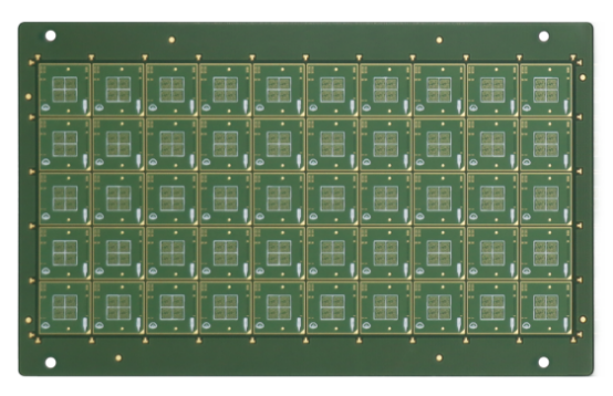
Introduction — Why Microstrip Impedance on IC Substrates Is Not the Same as PCB
Importance of Accurate Impedance in SI/PI/RF Design
Accurate impedance is fundamental to high-speed and high-frequency design because modern signals behave like controlled electromagnetic waves rather than simple voltage transitions. When the impedance of a transmission line deviates from its intended value, reflections occur along the channel. These reflections distort the signal, reduce the eye opening, increase jitter, and raise return loss. Even small mismatches can degrade the performance of standards such as PCIe, USB4, HDMI, or multi-gigabit SerDes links.
In packaging substrates, the tolerance for error is even tighter than in PCB. A deviation greater than 5% from the target impedance can cause system-level problems because the traces are shorter, operate at higher frequencies, and interact more strongly with surrounding dielectric materials. This means that a mismatch of just a few ohms may create enough reflection energy to exceed the allowable budget. As a result, achieving accurate impedance on IC substrates is not optional—it is critical to signal integrity, power integrity, and RF reliability.
Why PCB Tools Like Polar Si9000 Are Commonly Used
Polar Si9000 is widely used because it provides fast, convenient impedance calculations for traditional PCB stackups. The tool includes empirical models for common PCB materials, solder masks, and copper geometries. For PCB engineers, this means they can quickly enter trace width, spacing, dielectric thickness, and material properties to estimate characteristic impedance with good accuracy.
However, these PCB-oriented models do not fully represent IC substrate structures. Packaging substrates involve different dielectric materials, thinner build-ups, and additional layers such as molding compound. These layers significantly change the electromagnetic environment around a microstrip, but they are not included in most PCB calculators. As a result, Polar Si9000 may give a result that is correct for a PCB but inaccurate for a molded substrate. This limitation becomes clear when modeling top-layer microstrips in advanced packages, where the surrounding materials behave differently from traditional PCB air-interface structures.
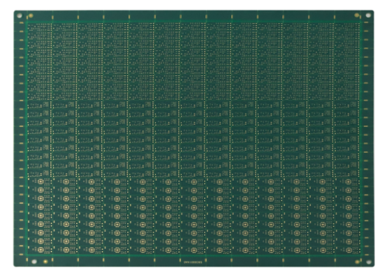
Structural Differences — PCB vs. IC Substrate in Microstrip Modeling
Why Stripline Modeling Works Well in IC Substrates
Stripline traces are fully embedded between two dielectric layers in a multilayer substrate. This configuration creates a uniform dielectric environment around the signal, which keeps the electromagnetic field confined. Because the surrounding material is consistent, the assumptions used for stripline impedance calculation in PCBs—such as homogeneous dielectric constants and predictable layer thicknesses—apply equally to IC substrates.
For example, a buried differential pair in a 6-layer packaging substrate behaves similarly to a buried pair in a multilayer PCB. The copper is completely surrounded by dielectric, reflections are minimal, and the calculated impedance closely matches reality. This is why PCB tools like Polar Si9000 can accurately model stripline structures in IC substrates without significant modifications.
Why Microstrip Modeling Is Fundamentally Different
Microstrip traces on IC substrates are not fully embedded. The top-layer copper is exposed to additional layers rather than open air, meaning the electromagnetic field interacts with multiple dielectric materials. Typically, the trace sits under a solder mask and is covered by a molding compound after packaging.
This changes the effective dielectric constant, which is the parameter that determines the trace’s characteristic impedance. For instance, air has a dielectric constant (Dk) of 1, but molding compounds typically have a Dk around 4, and solder mask ranges from 3.1 to 3.6. The higher Dk reduces the impedance compared to the PCB calculation that assumes an air interface. Ignoring these layers can easily lead to deviations of 5–10% in differential impedance.
Key Materials Involved
Solder Mask: A thin insulating layer applied to the top of the substrate to prevent short circuits and protect the copper. Its typical dielectric constant (Dk) is 3.1–3.6, and it slightly lowers the impedance of top-layer traces.
Molding Compound: A thick encapsulant used to protect ICs. It has a dielectric constant around 4 and a low loss factor (Df ≈ 0.01). Its presence above the traces significantly alters the electromagnetic field distribution and further reduces impedance.
Combined Effect vs. Air: A microstrip trace exposed only to air (Dk = 1) would have a higher characteristic impedance. When both solder mask and molding compound are present, the effective Dk increases, lowering the impedance and potentially causing mismatches if not modeled correctly.
In short, unlike fully embedded striplines, microstrips on IC substrates require careful consideration of all surrounding dielectric layers to accurately predict impedance and maintain signal integrity.
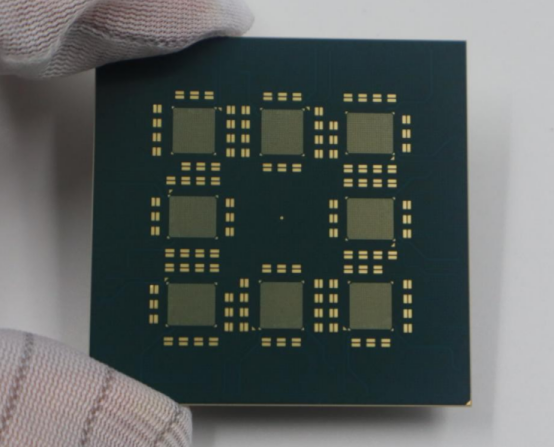
Case Study — 90Ω Differential Microstrip on a Packaging Substrate
Step 1 — Baseline Calculation Without Solder Mask or Molding Compound
As a starting point, we can model a 90Ω differential microstrip using Polar Si9000 with standard PCB-like assumptions. The input parameters include trace width, spacing, substrate thickness, and copper layer properties.
Using this simplified model, the calculated differential impedance is 90.75 Ω, which is very close to the target. However, this approach is overly idealized because it assumes the microstrip is exposed to air and does not account for the additional layers present in a real IC packaging substrate. In reality, the top-layer traces are covered by a solder mask and eventually encapsulated in molding compound, both of which change the effective dielectric constant around the trace.
Step 2 — Add Solder Mask to the Model
Next, we include the solder mask in the simulation. It is important to model the mask as a uniform layer rather than a “stair-step” approximation that some engineers assume. This produces a more realistic cross-section and more accurate field distribution.
With the solder mask included, the updated simulation shows the differential impedance drops to 87.49 Ω, representing a -3.6% deviation from the ideal 90.75 Ω. This demonstrates that even a thin layer of solder mask can meaningfully influence impedance and cannot be ignored in precise high-speed designs.
Step 3 — Add Molding Compound Above Solder Mask
Finally, the model incorporates the molding compound, typically 700 μm thick with a dielectric constant of Dk = 4. In this configuration, part of the microstrip’s electromagnetic field penetrates into the molding compound, further lowering the effective impedance.
Using Q2D simulation, the calculated differential impedance is approximately 83 Ω. This is an 8.5% reduction from the initial baseline, highlighting the significant impact of packaging materials on high-speed signal paths.
Clear Comparison Summary
Modeling Scenario
Impedance
Deviation vs Ideal
No mask + no molding
90.75 Ω
0%
With solder mask
87.49 Ω
-3.6%
With molding compound
83 Ω
-8.5%
Modeling Scenario | Impedance | Deviation vs Ideal |
|---|---|---|
No mask + no molding | 90.75 Ω | 0% |
With solder mask | 87.49 Ω | -3.6% |
With molding compound | 83 Ω | -8.5% |
Why This 8.5% Error Is Dangerous
An impedance deviation of 8.5% is comparable to typical fabrication tolerances and can have serious consequences for high-speed interfaces. Multi-gigabit protocols such as PCIe, USB4, DDR5, and SerDes links rely on precise impedance matching to maintain low reflection, minimal jitter, and a clean eye diagram. If the actual impedance falls to 83 Ω instead of the target 90 Ω, signal integrity can degrade, leading to bit errors, system instability, or even functional failure.
This case study underscores why accurate modeling of solder mask and molding compound is essential for modern packaging substrate design.
Why Polar Si9000 Cannot Model This Structure Correctly
Missing Ability to Stack Air/Mask/Molding Layers
Polar Si9000 is primarily designed for PCB impedance calculations, which assume standard surface and embedded layer structures. It works well when the microstrip or stripline is surrounded by a single uniform dielectric or a thin solder mask. However, IC packaging introduces a different scenario: the top-layer traces are covered by both a solder mask and a thick molding compound.
Polar Si9000 cannot fully represent this layered environment. The software lacks the ability to stack multiple dielectrics with widely differing dielectric constants (Dk) and thicknesses, such as Dk ≈ 4 for molding compound combined with a thin solder mask layer. As a result, the calculated impedance may match PCB expectations but can significantly deviate from the real value in a packaged IC substrate.
Frequency-dependent Dielectric Modeling Not Fully Accurate
Another limitation of Polar Si9000 is its simplified treatment of dielectric dispersion. Materials like molding compounds do not have constant dielectric properties—they exhibit frequency-dependent behavior, meaning the effective Dk changes with signal frequency. At higher frequencies, particularly above 2 GHz, this effect becomes pronounced.
Ignoring frequency-dependent variations can lead to further errors in impedance prediction. For instance, a 90Ω differential microstrip that appears correctly matched at low frequencies might drop to around 83Ω under actual high-frequency operation due to dispersion in the molding compound.
In short, while Polar Si9000 is convenient for PCB design, it cannot accurately model the complex material stack-up and frequency effects present in IC packaging. Designers need tools that account for multi-layer dielectrics and dispersive materials to ensure signal integrity, accurate differential impedance, and high-speed reliability.
Recommended Tools and Methods for Accurate IC Substrate Impedance Modeling
Q2D / Q3D (ANSYS)
Q2D and Q3D solvers from ANSYS are well-suited for modeling complex IC substrate microstrips because they can handle multi-layer dielectric stacks with high accuracy. Unlike PCB-oriented tools, these solvers allow engineers to define every layer, from the copper traces to the solder mask and molding compound, including their thicknesses and dielectric constants.
These tools use electrostatic and electromagnetic field solvers to calculate characteristic impedance, capturing the real behavior of fields around the trace. They can also visualize field penetration into the molding compound, helping engineers understand how the top-layer microstrip interacts with surrounding materials. This makes it possible to predict impedance changes and identify potential signal integrity issues before fabrication.
2.5D / 3D Solvers (HFSS, Clarity, Siwave)
For high-speed SerDes interfaces and multi-gigabit channels, full-wave solvers like HFSS, Clarity, or Siwave provide even more detailed modeling. These tools simulate frequency-dependent dielectric behavior, meaning they account for the fact that materials such as molding compounds exhibit dispersion at higher frequencies.
By supporting full-wave electromagnetic analysis, these solvers can capture complex interactions like crosstalk, reflection, and edge effects that simpler tools cannot. This level of precision ensures that the modeled impedance closely matches what will occur in the actual packaged IC, even in the 2 GHz+ range.
Best Practice Modeling Workflow
To ensure accurate impedance predictions, follow a structured workflow:
1. Extract the real stackup from the packaging team, including copper thickness, solder mask, and molding compound.
2. Include all dielectric layers in the simulation: copper → solder mask → molding compound.
3. Validate the model with cross-section measurements to confirm layer thickness and uniformity.
4. Sweep frequency during simulation to evaluate impedance variation across the operational range, capturing effects from dielectric dispersion and high-frequency interactions.
By following these steps and using advanced solvers, engineers can reliably predict microstrip impedance on IC substrates, reduce design iterations, and maintain signal integrity, low jitter, and proper differential matching for high-speed circuits.

Practical Design Guidelines for Packaging Substrate Microstrips
Always Include Molding Compound in Impedance Planning
For top-layer microstrip traces on packaging substrates, the molding compound must always be included in impedance calculations. Ignoring it leads to overestimation of impedance because the compound increases the effective dielectric constant around the trace. This is particularly important for high-speed signals, where even a few ohms of deviation can degrade signal integrity and increase reflections.
Rule of thumb: any top-layer microstrip that will be encapsulated must consider both solder mask and molding compound in the simulation.
When Can You Ignore Molding Compound?
There are specific scenarios where the molding compound has minimal impact:
Inner-layer striplines: fully embedded between dielectric layers, similar to traditional PCB multilayers, are largely unaffected by the molding compound above.
Very low-frequency applications (<100 MHz): at these frequencies, the effect of dielectric dispersion and field penetration into the molding compound is negligible, so impedance calculations are less sensitive to top-layer encapsulation.
These exceptions are useful for simplifying early-stage simulations but should be carefully validated before final design.
Achieving Target 90Ω Differential
To reach the desired 90Ω differential impedance, designers should:
1. Adjust trace width and spacing based on the measured dielectric constants of the actual stackup.
2. Consider solder mask openings, as partial exposure can slightly increase the effective impedance.
3. Re-validate the final model after packaging, using Q2D, 3D solvers, or cross-section measurements to ensure the predicted impedance matches the real fabricated substrate.
This iterative approach ensures that the design meets high-speed requirements while accounting for material and process variations.
Typical Tolerances for IC Substrate Manufacturers
Manufacturing introduces unavoidable variation that affects impedance:
Trace width control: typically ±2–3 μm, depending on line density and process.
Layer thickness variation: dielectric layers may vary ±5–10 μm, affecting field distribution.
Dielectric constant variation between lots: even small differences in molding compound Dk can shift impedance by several ohms.
When combined with modeling errors, these tolerances can lead to total impedance deviations comparable to 5–10%. Therefore, designers must consider both material tolerances and modeling accuracy to ensure reliable high-speed performance.
By following these guidelines, engineers can confidently design packaging substrate microstrips that meet differential impedance targets and maintain signal integrity across the entire operating frequency range.
Conclusion
Accurate impedance modeling on packaging substrates is essential for modern high-speed designs. Unlike traditional PCBs, IC substrates require careful consideration of the real material stackup, including solder mask and thick molding compound. Ignoring these layers can lead to deviations greater than 8%, potentially degrading signal integrity, increasing jitter, and impacting overall system reliability.
To achieve precise results, designers should rely on Q2D or full 3D solvers, which accurately capture multi-layer dielectrics, field penetration, and frequency-dependent behavior. Correct modeling ensures that differential impedance targets are met, maintaining the performance and reliability of high-speed interfaces such as PCIe, DDR5, or SerDes links.
At PCBMASTER, we combine precision manufacturing, advanced IC substrate materials, and professional simulation capabilities to deliver substrates that meet even the most stringent performance requirements. With AS9100 aerospace-grade certification, fine line width down to 25 μm, high-precision laser drilling, and full-process quality control, PCBMASTER ensures that every IC substrate is engineered for accuracy, reliability, and rapid production—from prototypes to small-batch custom solutions.
By integrating accurate impedance modeling with high-quality manufacturing, engineers can confidently design packaging substrates that perform as intended in demanding high-frequency applications.
FAQs
Why is microstrip impedance in IC substrates different from PCB?
Microstrip impedance on IC substrates differs because top-layer traces are covered by solder mask and molding compound, rather than being exposed to air like on PCBs. These additional dielectric layers increase the effective dielectric constant, lowering the impedance compared to PCB calculations. Unlike fully embedded striplines, the field around microstrips interacts with multiple materials, making accurate modeling critical.
Can Polar Si9000 accurately calculate impedance for packaging substrate microstrips?
Polar Si9000 works well for PCB stripline or microstrip structures, but it cannot fully model packaging substrates. It lacks the ability to stack multiple dielectrics like solder mask and thick molding compound and does not account for frequency-dependent behavior of materials. As a result, its impedance calculations for top-layer microstrips in IC packages can deviate significantly from reality.
How does molding compound affect differential impedance?
Molding compound has a dielectric constant around Dk = 4, which is higher than air (Dk = 1). When microstrip traces are encapsulated, part of the electromagnetic field penetrates into the molding compound, lowering the differential impedance. For example, a 90Ω target microstrip can drop to approximately 83Ω after molding, representing an 8.5% deviation if not properly modeled.
What tools are best for IC substrate impedance modeling?
Advanced solvers like Q2D, Q3D (ANSYS), HFSS, Clarity, and Siwave are recommended. These tools can:
Model complex multi-layer dielectrics including solder mask and molding compound.
Capture frequency-dependent dielectric behavior.
Perform full-wave electromagnetic simulation for high-speed signals.
They provide accurate impedance predictions and allow visualization of field penetration, which is essential for high-speed packaging design.
What is the acceptable impedance deviation for high-speed interfaces?
For high-speed interfaces such as PCIe, DDR5, USB4, and SerDes, impedance deviations larger than 5% can cause reflections, increased jitter, eye diagram closure, and potential system-level failures. Maintaining tight control within ±5% of the target impedance is critical for signal integrity (SI) and power integrity (PI) in IC packaging.