


How Ceramic PCBs Enhance Electronics: Key Materials & Manufacturing Processes Explained
As electronics continue to evolve, particularly in high-power and high-temperature environments, traditional PCB (Printed Circuit Board) materials are starting to show their limitations. To meet the increasing demands for superior thermal management, electrical insulation, and mechanical stability, ceramic PCBs have emerged as a top alternative. Offering exceptional thermal conductivity, high dielectric strength, and impressive mechanical robustness, ceramic PCBs are becoming the material of choice in industries ranging from LED lighting and power modules to electric vehicle (EV) inverters and aerospace applications.
However, not all ceramic materials are created equal. Different ceramics, such as Alumina (Al₂O₃), Aluminum Nitride (AlN), Silicon Carbide (SiC), and Zirconia (ZrO₂), each have unique characteristics that make them suitable for specific applications. Understanding the properties and advantages of these materials is key to choosing the right ceramic PCB for any given project.
In this article, we’ll explore the key materials used in ceramic PCBs, their distinct features, and the types of applications they’re best suited for. We’ll also dive into how ceramic PCBs work—covering their role in heat dissipation, electrical insulation, and mechanical stability. Finally, we’ll take a closer look at the manufacturing techniques that make ceramic PCBs a viable solution for high-performance electronics
Materials Used in Ceramic PCBs
In the world of ceramic PCBs, materials like alumina (Al₂O₃), aluminum nitride (AlN), silicon carbide (SiC), and zirconia (ZrO₂) offer various benefits for different applications. Alumina is cost-effective and works well in heat-sensitive electronics, while AlN excels in high-power applications requiring superior thermal management. SiC is unbeatable in extreme environments like aerospace, and zirconia provides flexibility for wearables and flexible PCBs. Each material is chosen based on its thermal, mechanical, and electrical properties, ensuring the right balance of performance and cost for every project.
By understanding the specific characteristics of each material, manufacturers can make informed decisions to optimize their products for both efficiency and longevity.
Alumina (Al₂O₃)
Properties:
Alumina, also known as aluminum oxide (Al₂O₃), is a highly durable and heat-resistant material. It has excellent thermal conductivity, meaning it can quickly spread heat, preventing overheating in electronic components. Alumina can handle high temperatures, making it suitable for maximum operating temperatures of up to 1,500°C, depending on the specific form used. In terms of cost-efficiency, alumina is one of the more affordable ceramic materials, offering a good balance between performance and price.
Applications:
Alumina is commonly used in LED lighting and power modules, where efficient heat dissipation is crucial. Its ability to withstand high temperatures and spread heat effectively makes it ideal for heat-sensitive electronics, such as those found in power supplies, amplifiers, and certain automotive applications. Alumina’s reliability and cost-effectiveness make it a preferred choice in industries where performance is essential, but cost must also be managed.
Aluminum Nitride (AlN)
Thermal Performance:
Aluminum nitride (AlN) is a highly thermally conductive ceramic material, which allows it to dissipate heat more efficiently than many other ceramics. This makes AlN ideal for applications that generate a lot of heat, as it helps to prevent overheating and damage to components. It also has a higher thermal conductivity than alumina, which improves heat management in electronic devices.
Applications:
AlN is widely used in EV inverters and high-power semiconductors, where heat management is crucial for performance and longevity. In these systems, AlN helps to prevent overheating of the components by efficiently transferring heat away from the active areas. Its high thermal conductivity also makes it a good choice for applications that require fast and reliable thermal management.
Cost Considerations:
While AlN offers excellent thermal performance, it is typically more expensive than alumina. This higher cost is a trade-off for its superior thermal properties. In situations where cost-efficiency is a priority, alumina may be chosen instead. However, for high-performance applications like power electronics and electric vehicles, the investment in AlN is often justified by its better heat management, which leads to longer-lasting and more reliable products.
Silicon Carbide (SiC)
Properties:
Silicon carbide (SiC) is known for its exceptional thermal conductivity and high-temperature resistance, which make it one of the toughest ceramic materials. SiC can handle extreme temperatures up to 1,600°C, making it perfect for environments that experience extreme heat. This material is not only heat-resistant but also offers mechanical strength and electrical insulation, which are crucial for specific applications in aerospace and power electronics.
Applications:
SiC is primarily used in aerospace, nuclear sensors, and other extreme environments where electronic components must operate under harsh conditions. For example, in space exploration or high-energy physics, where the environment can get incredibly hot or harsh, SiC ensures that the components remain stable and functional. It is also used in high-temperature electronics such as those in engines or other machinery exposed to heat.
Best Use Cases:
SiC’s high thermal conductivity and resistance to high temperatures make it an ideal material for high-temperature electronics. Devices such as power transistors in electric motors or sensors in industrial machinery, which require durability and efficiency under extreme temperature fluctuations, benefit greatly from SiC. SiC's unique properties make it a go-to material in industries that require performance at the highest operational temperatures.
Zirconia (ZrO₂)
Properties:
Zirconia (ZrO₂) stands out for its flexibility and toughness, making it an ideal material for applications requiring bending or movement. Unlike other ceramics that are rigid, zirconia can absorb mechanical stresses without cracking. It has a lower operating temperature tolerance compared to other ceramics, but its durability and flexibility make it useful for specific applications.
Applications:
Zirconia is commonly used in wearable devices and flexible ceramic PCBs. Its ability to bend without breaking is particularly important for products like smartwatches and medical implants, where the device needs to endure daily wear and tear. It’s also used in flexible electronic circuits, where flexibility is more important than high-temperature resistance.
Comparison Table
| Material | Properties | Applications | Best Use Cases |
| Alumina (Al₂O₃) | Durable, heat-resistant, good thermal conductivity, cost-effective | LED lighting, power modules, automotive applications, power supplies, amplifiers | Heat-sensitive electronics, cost-effective applications |
| Aluminum Nitride (AlN) | High thermal conductivity, efficient heat dissipation, more expensive than alumina | EV inverters, high-power semiconductors | High-performance power electronics, electric vehicles |
| Silicon Carbide (SiC) | Exceptional thermal conductivity, high-temperature resistance, mechanical strength | Aerospace, nuclear sensors, high-temperature electronics, industrial machinery | Extreme environments, high-temperature electronics |
| Zirconia (ZrO₂) | Flexible, tough, absorbs mechanical stresses, lower temperature tolerance | Wearable devices, flexible PCBs, medical implants | Flexible electronics, wearable tech, medical devices |
How Ceramic PCBs Work
Ceramic PCBs are an essential part of modern electronics, offering efficient thermal management, high electrical insulation, and mechanical stability in harsh environments. The combination of excellent heat dissipation, high dielectric strength, and resistance to thermal expansion makes them ideal for high-performance applications. Whether it’s in power modules, LED drivers, or automotive sensors, ceramic PCBs offer unmatched reliability and longevity. These characteristics allow them to excel in environments where traditional materials like FR4 would fail, making them a crucial component in industries requiring high heat tolerance, electrical safety, and mechanical durability.
Efficient Thermal Pathways
Heat Dissipation:
One of the primary reasons ceramic PCBs are used in electronics is their excellent heat dissipation abilities. Ceramic materials, like alumina (Al₂O₃) and aluminum nitride (AlN), can quickly transfer heat away from sensitive components, preventing them from overheating. This happens because ceramic substrates have high thermal conductivity, meaning heat moves through them much faster than through traditional materials like FR4 (the standard material for most PCBs).
In comparison, FR4 PCBs are less effective at spreading heat. FR4 is made of glass fibers and epoxy resin, which are not as efficient at transferring heat. This can lead to components running hotter and potentially failing due to heat buildup. In contrast, ceramic PCBs can keep components cooler for longer, enhancing the reliability of power modules, LED lighting, and other heat-sensitive devices.
Thermal Path Efficiency:
Ceramic PCBs not only dissipate heat quickly but also ensure thermal path efficiency. This means that the heat transfer process is more streamlined, leading to enhanced performance and reliability in high-heat applications. When electronic components are exposed to constant heat, their performance can degrade over time. By using ceramic materials with efficient thermal pathways, electronics are protected, extending their lifespan and reducing the risk of thermal damage. For instance, power modules used in electric vehicles (EVs) rely on ceramic PCBs to maintain performance under high-heat conditions.
Electrical Insulation & Voltage Management
Dielectric Strength:
Another key benefit of ceramic PCBs is their dielectric strength, which refers to the material's ability to withstand electrical stress without breaking down. Ceramic materials have a dielectric strength greater than 20 kV/mm. This is particularly useful in power applications, where high voltages are involved. Materials with high dielectric strength ensure that the PCB can safely manage the electrical signals without causing short circuits or failures. For example, in power supplies or high-voltage circuits, ceramic PCBs are used to insulate and protect sensitive components from electrical overloads, ensuring stable performance.
Current Leakage Prevention:
Ceramic materials also play a critical role in preventing current leakage. In high-voltage systems, current leakage can lead to arcing, short circuits, or even fires. Ceramic PCBs are highly resistant to electrical leakage due to their excellent insulation properties. This makes them ideal for high-voltage applications like LED drivers, solar inverters, and electrical vehicles, where electrical safety is paramount. For instance, in solar power inverters, ceramic PCBs prevent electrical leakage that could damage the system or cause safety hazards, thus enhancing the overall reliability of the system.
Mechanical Stability in Harsh Environments
Low CTE Advantages:
One of the standout features of ceramic PCBs is their low coefficient of thermal expansion (CTE). CTE refers to how much a material expands or contracts when exposed to temperature changes. Ceramic materials have a low CTE, which means they don’t change size much with temperature fluctuations. This is especially important in thermal cycling – where the PCB is repeatedly exposed to high and low temperatures. PCBs with low CTE are more resistant to cracking and warping, even under extreme heat or cold. This property makes ceramics more reliable than materials like FR4 in environments where temperature changes are frequent.
For example, in automotive electronics, parts like engine control units (ECUs) are exposed to constant changes in temperature. Using ceramic PCBs in such applications helps maintain structural integrity and prevents the PCB from cracking or losing connection during thermal cycles.
Resistance to Mechanical Stresses:
Ceramic PCBs are also resistant to mechanical stresses, such as vibration, shock, and impact. This is crucial for industries like aerospace, automotive, and industrial machinery, where components are often subjected to harsh physical conditions. Unlike traditional PCBs, ceramic materials can endure high levels of vibration and impact, making them ideal for applications like automobile sensors or space electronics, which require durability in extreme environments.
Durability in Harsh Conditions:
The overall durability of ceramic PCBs makes them the preferred choice for electronics in harsh conditions. They can withstand not only temperature extremes but also chemical exposure, mechanical stress, and radiation. This makes ceramic PCBs suitable for use in demanding sectors such as aerospace, where components must endure high speeds, radiation, and temperature extremes. They are also used in heavy industrial machinery, where reliability and long-lasting performance are critical.
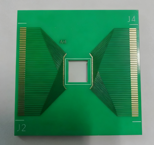
Manufacturing Ceramic PCBs: Key Techniques
The manufacturing techniques for ceramic PCBs—such as Direct Bonded Copper (DBC), Active Metal Brazing (AMB), Thick Film Technology, and Laser Direct Structuring (LDS)—each offer unique advantages suited to specific applications.
Each technique is tailored to meet the demands of various industries, from automotive to consumer electronics. Understanding these techniques allows manufacturers to choose the best option for their specific needs, optimizing both performance and cost-efficiency.
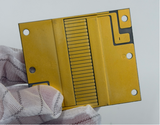
Direct Bonded Copper (DBC) Process
Step-by-Step Process:
The Direct Bonded Copper (DBC) process involves bonding copper directly to a ceramic substrate, typically made of alumina (Al₂O₃) or aluminum nitride (AlN). First, a layer of copper foil is placed on the ceramic surface, and then the copper is bonded using a high-temperature process. The heat causes the copper to fuse directly to the ceramic, creating a solid bond that ensures high thermal conductivity and electrical performance. The bonding process helps ceramic PCBs efficiently handle the heat produced by high-power components, preventing failure due to overheating.
Applications:
The DBC process is commonly used in high-power modules and heat-sensitive electronics. These include power modules in electric vehicles (EVs), LED lighting, and industrial power supplies. These applications require effective heat dissipation, and DBC helps maintain component performance by ensuring thermal management.
Benefits and Limitations:
Benefits: DBC provides high thermal and electrical conductivity, which helps in managing heat in high-power applications. The copper layer allows for efficient heat transfer, ensuring the components stay cool and operate reliably.
Limitations: One limitation of the DBC process is its difficulty with flat substrates. The process works best when the ceramic is flat and uniform, so it may not be suitable for more complex or 3D designs. Additionally, DBC bonding can be expensive, especially for small production runs.
Active Metal Brazing (AMB) Process
Overview:
The Active Metal Brazing (AMB) process is used to create strong, reliable connections between ceramics like aluminum nitride (AlN) or silicon carbide (SiC) and metals. In AMB, a metal is melted and applied to the ceramic surface, creating a strong bond. The active metal reacts with the ceramic surface, allowing the metal to bond tightly, even in high-temperature environments. This process ensures that the ceramic and metal can work together efficiently in high-power and high-temperature applications.
Applications:
AMB is commonly used in high-temperature, high-reliability applications. Examples include power electronics, electric vehicle inverters, and industrial machinery. These industries need ceramic materials that can withstand extreme temperatures while maintaining strong metal connections, making AMB the ideal choice.
Pros and Cons:
Pros: AMB offers enhanced thermal and mechanical performance. The bond created is highly durable, ensuring long-lasting connections in high-stress environments. This makes it suitable for demanding applications where reliability is critical.
Cons: The AMB process can be costly and challenging to perform with high precision, especially when working with complex or small-scale designs. The process requires high-quality materials and careful control of temperature and pressure, which can increase production costs.
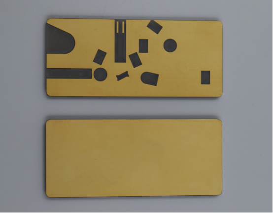
Thick Film Technology
Printing Process:
Thick Film Technology involves using conductive inks to print resistors, traces, and other electrical components directly onto a ceramic substrate. The inks are made from a combination of metals (such as silver or gold) and glass, which, when fired at high temperatures, form solid electrical paths. This process is particularly useful for creating precise, low-power ceramic PCBs that require customized components.
Applications:
Thick film technology is typically used for sensors and low-power electronic devices, such as those found in medical equipment, automotive sensors, and home appliances. These applications do not require the high thermal management of power electronics but still need reliable, precise electrical connections.
Benefits:
Precision: Thick film technology allows for precise patterns and high accuracy, which is crucial for creating small, detailed circuits.
Cost-efficiency: It is a more cost-effective method for producing ceramic PCBs in low-volume runs compared to other methods like DBC or AMB.
Flexibility: The process can be adapted to create custom components, allowing for design flexibility in a wide range of applications.
Laser Direct Structuring (LDS) for 3D PCBs
Laser Activation and Copper Plating:
Laser Direct Structuring (LDS) is a process used to create 3D circuit structures on ceramic substrates. First, the ceramic surface is laser-activated, which creates tiny, conductive areas on the substrate. Then, copper is plated onto these activated areas, forming electrical traces. This process allows for the creation of complex, 3D PCBs that can be used in applications requiring more intricate designs, such as high-density interconnects (HDI).
Use Cases:
LDS is ideal for creating flexible and complex PCBs used in modern electronics. For example, smartphones, wearable devices, and flexible displays all require 3D PCBs to handle advanced features like multi-layer connections and space-saving designs. LDS helps in creating compact and high-performance PCBs that fit into small or flexible spaces.
Applications:
LDS is widely used for high-density interconnect (HDI) boards and 3D printed circuit boards (PCBs). These applications require a PCB that is not only compact but also capable of handling complex, multi-layer connections that traditional 2D PCBs cannot. This is particularly useful in industries like consumer electronics, medical devices, and aerospace, where the demand for space-efficient and high-performance components is high.
Conclusion
In conclusion, ceramic PCBs are essential for high-power, high-temperature, and flexible applications across industries like automotive, aerospace, and electronics. Their ability to manage heat, offer strong electrical insulation, and remain stable in harsh environments makes them the ideal choice for demanding applications.
Looking to the future, ceramic PCB technology will continue to evolve, with a focus on miniaturization and 3D designs to support the growth of sectors like consumer electronics, electric vehicles, and renewable energy.
For those seeking high-quality ceramic PCBs, PCBMASTER is a leading provider with over 10 years of expertise. Specializing in advanced ceramic substrates like alumina (Al₂O₃), aluminum nitride (AlN), and silicon nitride (Si₃N₄), PCBMASTER delivers tailored solutions for high-performance, high-reliability applications. Their commitment to innovation and quality ensures that they can meet the demanding needs of industries requiring top-tier electronic components.
FAQs
Why are ceramic PCBs preferred for high-power applications over traditional FR4 PCBs?
Ceramic PCBs are preferred for high-power applications due to their superior thermal conductivity and high-temperature resistance. Unlike traditional FR4 PCBs, which have limited heat dissipation capabilities, ceramic substrates can handle higher thermal loads, reducing the risk of overheating and ensuring reliable operation in demanding environments. Ceramic materials like aluminum nitride (AlN) and silicon nitride (Si₃N₄) can efficiently dissipate heat, extending the lifespan of high-power electronic components.
What makes laser direct structuring (LDS) a suitable technique for creating 3D ceramic PCBs?
Laser Direct Structuring (LDS) is ideal for creating 3D ceramic PCBs because it allows for precise and flexible design. The process uses a laser to activate specific areas of the ceramic substrate, which are then plated with copper to form conductive paths. This method enables the production of complex, multi-layered circuits in compact, space-efficient designs, which are essential for modern electronics like wearable devices and high-density interconnects (HDI). LDS also supports the growing demand for flexible and high-performance electronics.
How does the Active Metal Brazing (AMB) process improve the reliability of ceramic PCBs in extreme environments?
The Active Metal Brazing (AMB) process enhances the reliability of ceramic PCBs by creating strong, durable bonds between metal and ceramic materials. In high-temperature and high-stress environments, such as aerospace and electric vehicle applications, AMB ensures that the metal-ceramic interface remains intact, preventing thermal expansion mismatches or material degradation. This results in improved thermal conductivity and mechanical stability, making AMB a key technique for high-reliability applications where performance under extreme conditions is critical.

