


Bare Printed Circuit Board Design Guidelines for Better Performance
When we build modern electronics, even a very small mistake in the circuit board design can cause big problems. Signals might get weaker, parts may get too hot, or the product might not work well at all.
Many engineers want faster speed, smaller size, and stronger reliability. But they often forget one important thing: the design of the bare PCB — the empty board before parts are added.
If we follow clear design rules from the very beginning, we can make sure the final device is stable, safe, and not too expensive.
In this guide, I’ll share easy-to-follow rules for designing bare printed circuit boards (bare PCBs). These rules cover materials, layers, wiring, and surface finishes. By using them, you can build boards that work better and last longer.
What Is a Bare Printed Circuit Board?
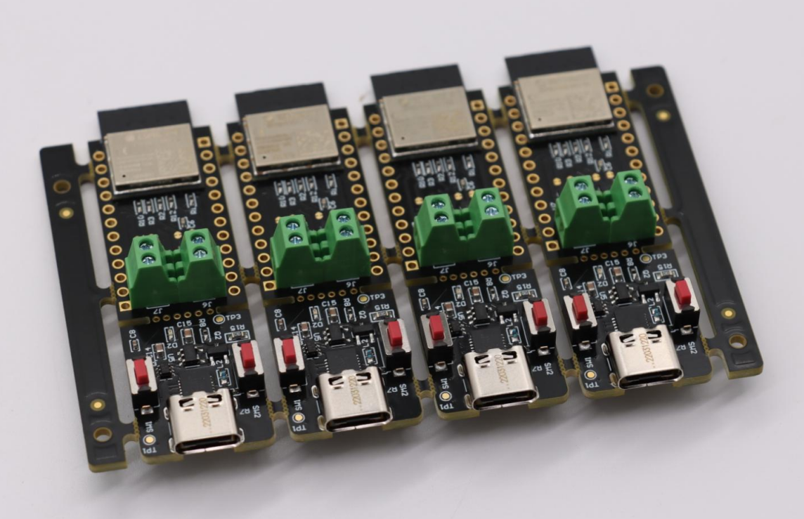
Let’s start with the basics. A bare printed circuit board, or bare PCB, is the board you see before any electronic parts are put on it. It’s like the empty foundation of a house — the floor, the walls, and the wiring paths are there, but the furniture and lights are not added yet.
The board is usually made of a hard material, like fiberglass, with thin copper lines on it. These copper lines act like “roads” for electricity, guiding signals from one place to another.
Why is a bare PCB important?
In electronics manufacturing, the bare PCB is the starting point. Without it, we cannot connect chips, resistors, capacitors, or any other parts. The bare PCB gives shape and order to the whole system. It makes sure electricity can travel the right way, safely and reliably.
Think of it like this: if you want to build a city, you first need roads and blocks. Only then can you add houses, shops, and cars. The bare PCB works the same way for electronic devices.
Bare PCB vs. PCBA
Now, what’s the difference between a bare PCB and a PCBA?
A bare PCB is just the empty board — no parts, only copper lines.
A PCBA (Printed Circuit Board Assembly) is when we take that empty board and add all the components on top, like chips, connectors, and other devices.
So you can remember it this way:
Bare PCB = the blank board
PCBA = the finished, working board
Without the bare PCB, there is no PCBA. It’s the first and most important step in making any electronic product.
Main Goals of Bare PCB Design
When we design a bare printed circuit board, there are three main goals we always keep in mind. These are performance, reliability, and cost. By focusing on these goals, we can make sure the board works well, lasts longer, and stays within budget.
1. Better Performance
A well-designed PCB allows electrical signals to travel smoothly and quickly. If the board has low resistance, the electricity flows more easily, just like cars moving faster on a wide, clean road. At the same time, the design should reduce noise, so that signals do not get mixed up or disturbed. When performance is high, the electronic device becomes faster, more stable, and more efficient.
2. Strong Reliability
This means it should work the same way every time without failing. A good design reduces mistakes during manufacturing, which means fewer defective boards. In other words, more boards pass the quality test and fewer end up in the trash. This is very important because unreliable boards can cause bigger problems later, such as product recalls or repairs. By designing for reliability from the start, we can save time, money, and effort in the long run.
3. Cost Control
High-performance boards often use better materials and extra layers, but this makes them more expensive. On the other hand, very cheap materials may lower the cost, but they can also lower the quality and performance of the board. The challenge is to find a balance between performance and budget. A smart design gives the customer good value: strong performance at a fair price. It’s like buying shoes — you don’t always need the most expensive pair, but you also don’t want a pair that breaks after one week.
Bare PCB Design Guidelines
Designing a bare printed circuit board is like building the foundation of a house. A strong, well-planned foundation supports everything above it. If the foundation is weak or poorly designed, problems will show up later. Here are detailed guidelines for making better bare PCBs.
1. Material Selection (Substrate & Copper)
Substrate materials: The substrate is the main material of the board and holds everything together. Common options include FR4, which is strong, cheap, and works for most electronic devices, and Rogers, which is better for high-speed or high-frequency applications but costs more. Using the right substrate helps signals move smoothly and reduces the chance of overheating or interference.
Copper thickness: Copper forms the pathways for electricity on the board. Thicker copper can carry more current and helps the board release heat better, which is important for devices with high power. Thinner copper is cheaper and easier to work with, but it may overheat or fail if too much current passes through. Choosing the right thickness depends on the type of device and how much current it will carry.
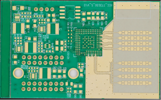
2. Layer Stack-Up
Multi-layer benefits: PCBs can have one layer, two layers, or many layers stacked together. Multi-layer boards allow designers to separate signal paths from power and ground layers. This separation reduces electrical noise, prevents signals from interfering with each other, and makes the board more stable.
Stack-up strategies: A typical approach is to place power and ground planes in the middle of the board and signal layers on the outside. This configuration reduces electromagnetic interference, keeps signals clean, and ensures the board works reliably even at high speeds. Proper stack-up planning also makes it easier for manufacturers to build the board correctly.
3. Trace Design
Trace width and spacing: Traces are the copper lines connecting components. The width and spacing of traces are very important. Thin traces can overheat or even burn out when too much current flows. If traces are too close together, electrical signals may leak from one to another, causing errors or interference. Engineers must carefully calculate the width and spacing based on current and voltage levels.
Impedance control: For high-speed signals, controlling impedance is essential. Impedance is like the “resistance” to signals moving along a trace. If it is not controlled, signals can reflect or weaken, causing devices to malfunction. Engineers design traces with precise widths, distances, and materials to keep impedance stable.
Power and ground layout: Good placement of power and ground traces reduces electrical noise and ensures that the device receives stable voltage. Poor layout can cause signal drop, interference, or even damage components over time.
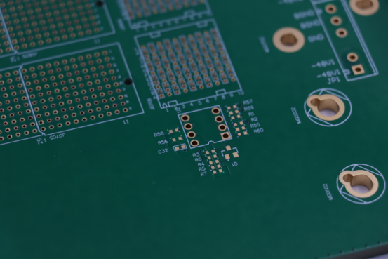
4. Vias and Pads Design
Types of vias: Vias are small holes that connect different layers of a PCB. There are through-hole vias, which go from the top to the bottom layer; blind vias, which connect an outer layer to an inner layer; and buried vias, which only connect inner layers. Using the right type of via saves space, improves performance, and allows for more complex designs.
Pad size and reliability: Pads are small metal areas where components are soldered. Pads that are too small make soldering difficult and weak. Pads that are too large may cause components to sit incorrectly or short-circuit with nearby traces. Proper pad design ensures strong mechanical connections and long-term reliability of the PCB.
5. Surface Finish
Common finishes: The copper on a PCB can oxidize, which makes soldering hard. To prevent this, we use surface finishes. Common options include ENIG (Electroless Nickel Immersion Gold), which is smooth, durable, and perfect for fine-pitch components; OSP (Organic Solderability Preservatives), which is cheaper and works for standard boards; and HASL (Hot Air Solder Leveling), which is widely used for general applications.
Impact on quality: The choice of surface finish affects how easy it is to solder parts and how reliable the board will be over time. ENIG lasts longer and works well for high-end devices. OSP is cheaper but can wear out faster. HASL is practical for many standard applications but may be uneven for very small parts.
6. Design for Manufacturability (DFM)
Work with manufacturers: Every PCB manufacturer has limits, such as the smallest hole size or the thinnest trace they can make. Ignoring these limits can make a board impossible or expensive to produce. Engineers should discuss design plans with manufacturers early to avoid problems.
Key parameters: Important factors include tolerances, minimum spacing between traces, and minimum hole size. Following these rules ensures the board can be built reliably and reduces the risk of defects.
Balance of design and cost: Good DFM design makes the PCB easier to manufacture, saves money, and increases the chance that all boards will pass quality checks. A well-balanced design considers both performance and cost, making the final product both reliable and affordable.
Common PCB Design Mistakes and How to Avoid Them
Even experienced engineers can make mistakes when designing PCBs. Small errors can cause big problems in performance, reliability, and cost. Here are some common mistakes and how to avoid them.
1. Traces Too Long or Irregular
If the copper traces on a PCB are too long or follow irregular paths, signals may travel slower or get distorted. This is called signal delay.
To avoid this, plan trace paths carefully. Keep them as short and direct as possible. Use smooth curves instead of sharp angles, and try to run high-speed signals on dedicated layers with proper ground support. Short, clean traces help signals travel faster and more reliably.
2. Ignoring Heat Management
Some boards carry a lot of electrical current, which generates heat. If the design does not consider heat dissipation, components may overheat, causing the board to fail or behave poorly.
To prevent this, include wide traces for high-current paths and use copper planes to spread heat. Add thermal vias to move heat from hot spots to other layers, and make sure sensitive components are placed in areas with good airflow. Proper heat management keeps the board stable and extends its life.
3. Not Considering Manufacturing Limits
Every factory has rules about the smallest traces, minimum spacing, and hole sizes. Ignoring these limits can make the board impossible to build, or force expensive rework.
To avoid this, talk to your manufacturer before finalizing the design. Make sure all trace widths, hole sizes, and spacing meet the factory’s capabilities. Designing with manufacturability in mind saves money, time, and frustration.
Conclusion
Following proper bare PCB design rules is the key to making boards that work well and last longer.
By carefully choosing materials, arranging layers, designing traces, and selecting the right surface finish, you can get the best performance from your board.
Working with experienced manufacturers, like PCBMASTER, helps turn your design into a high-quality, reliable finished product.
FAQs
1. Why is copper quality important for a bare PCB?
Copper is the material that carries electricity on the PCB. If the copper is poor quality, it can have tiny cracks or uneven surfaces. This can make signals weaker, cause overheating, or even short circuits. Good copper ensures the board works reliably and lasts longer. It also makes soldering components easier and safer.
2. Can a bare PCB be reused if a mistake is made?
Usually, bare PCBs are not reusable once a serious mistake is made, like a broken trace or damaged pad. Fixing them can be very hard and sometimes impossible. That’s why careful design and checking before manufacturing is very important. A well-planned board reduces waste and saves money.
3. How does PCB size affect its performance?
The size of the PCB matters for signal speed, heat, and component placement. Smaller boards can be faster because signals travel shorter distances, but they can get crowded, which increases the chance of interference or overheating. Larger boards have more space for traces and heat management but may cost more. Choosing the right size is a balance between performance, reliability, and cost.

