


Advanced Assembly PCB: Complete Guide to High-Quality Boards
Looking for a reliable way to build complex, high-performance circuit boards? This guide explains what advanced assembly PCB is, its key features, and why it matters for modern electronics.
What Is Advanced Assembly PCB?
Definition and Key Features
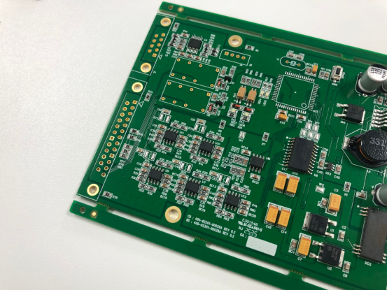
Advanced assembly PCB refers to the process of building printed circuit boards that go beyond basic 2-layer designs. These boards often include:
l Multi-layer stackups (4–20+ layers) for complex routing and high-speed signals
l HDI (High-Density Interconnect) features like microvias, blind and buried vias
l Fine-pitch component placement such as BGA, QFN, and 01005 passives
l Precision-controlled impedance for RF and high-frequency applications
Compared to standard PCB assembly, advanced assembly requires tighter tolerances, more sophisticated equipment, and specialized expertise. Standard assembly may only handle basic SMT components on a 2-layer board, while advanced assembly can manage high-density circuits with hundreds of components placed in a very small area.
Example:
l A 2-layer hobby PCB might just have through-hole resistors and DIP ICs, soldered by hand.
l A 10-layer high-frequency board may route differential pairs for high-speed data, use microvias for signal integrity, and require X-ray inspection for hidden BGA joints.
This difference is what makes advanced assembly crucial for high-reliability, compact, and performance-critical electronics.
Why Advanced Assembly PCB Matters for Modern Electronics
Modern devices demand smaller, faster, and more reliable circuit boards. Advanced PCB assembly makes this possible by supporting:
l Miniaturization – fits more functionality into a smaller footprint, essential for smartphones, wearables, and IoT devices.
l High-speed performance – maintains signal integrity for gigahertz-level communication and computing.
l Durability and reliability – uses precise soldering and thorough inspection to reduce field failures.
Key Applications:
l Medical devices – where space and reliability are critical (e.g., portable diagnostic tools).
l Industrial controls – where PCBs must withstand harsh environments and run 24/7.
l IoT hardware – compact, power-efficient boards for connected devices.
In short, advanced assembly PCB enables next-generation electronics by combining complex design, high precision, and rigorous quality control.
Types of Advanced Assembly PCB
Surface Mount Technology (SMT) Assembly
Surface Mount Technology (SMT) is the most common method for advanced PCB assembly. Components are mounted directly onto the board surface rather than using through-hole leads.
Step-by-step SMT process:
l Solder Paste Printing – A stencil applies solder paste to the pads where components will sit.
l Pick-and-Place – Automated machines place resistors, capacitors, ICs, and other parts onto the paste-covered pads.
l Reflow Soldering – The board passes through a reflow oven, melting the solder and securing the components in place.
l Inspection – Automated Optical Inspection (AOI) checks for misaligned or missing components.
Benefits of SMT Assembly:
l Allows compact and lightweight PCB designs.
l Supports high-speed automated production, improving consistency and reducing labor costs.
l Enables high component density, ideal for smartphones, IoT devices, and high-speed circuits.
Through-Hole Assembly
Through-hole assembly involves inserting component leads into drilled holes and soldering them from the opposite side.
When it is still needed:
l High-power components such as transformers, inductors, or large connectors.
l Mechanical strength applications where components must withstand vibration or stress.
Pros vs. SMT:
l Pros: Stronger mechanical bond, better for power components, more heat-tolerant.
l Cons: Takes more space, less suitable for miniaturized designs, slower assembly process.
Mixed Technology Assembly
Some PCBs require both SMT and through-hole components. This is known as mixed technology assembly.
Use cases:
l Power boards that need SMT control circuits plus large through-hole connectors.
l Communication modules that combine surface-mount RF chips with robust pin headers.
Example: A power supply board might have surface-mount ICs controlling voltage regulation while using through-hole capacitors for energy storage.
Special Processes
Advanced PCBs often involve specialized assembly techniques beyond basic SMT or through-hole.
Key special processes:
l BGA (Ball Grid Array) & QFN packages – require X-ray inspection because solder joints are hidden under the package.
l Micro-BGA handling – supports extremely fine-pitch components for high-density designs.
l Controlled impedance assembly – ensures consistent signal integrity for high-frequency or differential pair routing.
l Fine-pitch assembly – precise placement for 0.4 mm pitch components or smaller.
These processes ensure signal reliability and miniaturization in complex designs such as high-speed networking boards and compact medical devices.
Key Steps in Advanced PCB Assembly Process
Design for Manufacturability (DFM)
Design for Manufacturability (DFM) is the first and most important step in advanced PCB assembly. DFM checks ensure your design can be built reliably and cost-effectively.
Why DFM is critical:
l Prevents costly rework and production delays.
l Identifies design issues early, before fabrication begins.
Common issues detected in DFM reviews:
l Spacing violations – traces or pads too close together.
l Via placement problems – vias under components causing solder wicking.
l Component clearance issues – parts placed too close for pick-and-place machines.
By running a DFM check, engineers can adjust the design and guarantee smooth production.
PCB Fabrication
Once the design passes DFM, PCB fabrication begins.
Key steps in PCB fabrication:
l Board stack-up planning – defines the number of layers, material type, and copper thickness.
l Controlled impedance design – critical for high-speed signal integrity.
l Drilling and plating vias – including microvias for HDI boards.
l Final finishing – surface finish selection (ENIG, HASL, OSP) for solderability.
Example: An 8-layer high-speed PCB might use a stack-up with signal-ground-signal pairs to reduce crosstalk, plus controlled impedance traces for differential pairs.
Component Sourcing
Reliable component sourcing is key to meeting production schedules.
Best practices for component sourcing:
l Use an Approved Vendor List (AVL) to ensure part quality and traceability.
l Plan for shortage management by qualifying alternate parts early.
l Work with suppliers who can guarantee authenticity and provide certificates of conformity.
Benefit of turnkey solutions:
Turnkey assembly services handle procurement, reducing your workload and avoiding sourcing delays. This approach is ideal for prototypes and production runs alike.
Assembly & Soldering
This step mounts components onto the fabricated PCB.
Typical assembly flow:
1. Solder paste printing – applies paste to the pads.
2. Pick-and-place – automated placement of components.
3. Reflow soldering – melts solder to secure SMT parts.
4. Wave soldering or selective soldering – used for through-hole components in mixed assemblies.
Inspection:
l AOI (Automated Optical Inspection) checks component orientation and placement.
l X-ray inspection verifies hidden solder joints under BGA or QFN packages.
These inspections ensure assembly quality before testing.
Testing & Quality Control
Testing verifies that every assembled PCB functions correctly.
Common PCB testing methods:
l ICT (In-Circuit Test): Checks individual components and connections.
l Flying Probe Test: Ideal for prototypes or low-volume production.
l Functional Test: Simulates real-world operation to confirm performance.
Why 100% E-Test matters:
Electrical testing of every board ensures there are no shorts, opens, or continuity issues—critical for safety and reliability in demanding applications.
Benefits of Advanced Assembly PCB
Higher Performance & Reliability
Advanced PCB assembly delivers better signal integrity thanks to precise impedance control, optimized routing, and accurate component placement. This reduces noise, crosstalk, and signal loss in high-speed circuits.
Key reliability benefits:
l Lower defect rates: Automated optical inspection (AOI) and X-ray verification catch defects early.
l Reduced field failures: High-quality solder joints and thorough testing minimize product returns.
l Longer product life: Reliable assembly means fewer intermittent faults in demanding environments.
Example: A telecom board using micro-BGA packages can maintain stable data transfer rates with fewer failures compared to a low-precision assembly line.
Faster Time-to-Market
In competitive industries, speed is critical. Advanced assembly processes enable parallel workflows where PCB fabrication, component sourcing, and stencil preparation happen simultaneously.
Benefits for time-to-market:
l Rapid prototyping: Quick-turn PCB assembly helps engineers validate designs faster.
l Prototype-to-production scalability: The same assembly line can move from a few test boards to full-scale production without redesigning the process.
l Reduced lead time: Integrated sourcing and manufacturing cut delays caused by supply chain bottlenecks.
This allows companies to launch products ahead of competitors, capturing market share sooner.
Cost Efficiency in Complex Projects
Although advanced PCB assembly may have a higher upfront cost, it often saves money in the long run.
Ways it reduces total cost:
l Lower rework and scrap rates: Fewer production defects mean less wasted material and labor.
l Improved yield: High-precision processes increase first-pass success rates.
l Better total cost of ownership: Quality assembly prevents expensive warranty claims and field failures.
Comparison: A cheap assembly shop might offer lower pricing but can lead to higher failure rates, delays, and rework costs—resulting in a more expensive project overall.
Common Challenges of Advanced Assembly PCB and How to Solve Them
Component Shortages
Component shortages are one of the most common obstacles in PCB assembly. Global supply chain issues, part obsolescence, or sudden demand spikes can delay projects.
Effective strategies to handle shortages:
l Alternate part selection: Identify equivalent components early and keep a list of approved substitutes.
l Lifecycle management: Track part lifecycles to avoid using obsolete or near end-of-life components.
l Strategic sourcing: Work with suppliers who offer real-time inventory visibility and secure supply agreements.
Example: If a specific microcontroller is out of stock, engineers can redesign around a pin-compatible alternative to keep production on schedule.
Assembly Defects
Even with precision equipment, assembly defects can occur if processes are not optimized.
Common defects include:
l Tombstoning: Small components like resistors lift from one pad during reflow.
l Solder bridging: Excess solder connects two adjacent pads, creating shorts.
l Voiding: Air pockets in solder joints that reduce reliability.
Preventive measures:
l Proper stencil design: Control solder paste volume to reduce bridging and tombstoning.
l Reflow profile optimization: Adjust temperature profiles to ensure smooth solder melting and solidification.
l AOI and X-ray inspection: Detect defects early and reduce rework costs.
Design Complexity
Complex PCB designs can create manufacturability challenges if not planned correctly.
Tips to manage design complexity:
l Early manufacturer involvement: Share design files with your assembly partner during the layout stage for feedback.
l DFM review: Run Design for Manufacturability checks to spot spacing violations, via issues, and component clearance problems before fabrication.
l Standardization: Use commonly available component packages and consistent design rules to simplify production.
Example: An early DFM review might flag a via-in-pad design that would trap solder, allowing the designer to switch to filled vias before production.
How to Choose the Right Advanced PCB Assembly Partner
Capabilities to Look For
When selecting an advanced PCB assembly partner, it is essential to evaluate the technical capabilities of the manufacturer.
Key capabilities include:
l Minimum pitch size support: Ability to handle fine-pitch components like 0.4 mm or smaller.
l BGA and QFN support: Expertise in placing and soldering ball grid arrays and quad flat no-leads packages.
l X-ray inspection: Ensures hidden solder joints are defect-free.
l Certifications: ISO 9001 for quality management, IPC-A-610 for assembly standards, and RoHS compliance for environmental safety.
These capabilities ensure the manufacturer can handle complex, high-density, and high-reliability PCB designs.
Quality and Traceability
High-quality assembly requires rigorous tracking and documentation throughout production.
Key practices for quality and traceability:
l Batch tracking: Records every step of production for each board lot.
l Process documentation: Maintains assembly procedures, inspection results, and test reports.
l Case study example: A high-speed networking PCB showed a 15% yield improvement after switching to a partner that implemented full traceability, reducing rework and scrap.
Proper traceability allows fast root-cause analysis if issues arise, minimizing production delays and warranty risks.
Communication and Support
Effective collaboration with your PCB assembly partner can significantly improve project outcomes.
Benefits of strong support:
l Engineering support: Helps optimize design for manufacturability and assembly efficiency.
l Rapid prototyping services: Accelerates time-to-market by quickly producing functional prototypes for testing.
l Transparent communication: Clear updates on production status, material availability, and testing results reduce misunderstandings and delays.
Recommendation: PCBMASTER is a trusted advanced PCB assembly partner offering high-quality manufacturing, full traceability, and responsive engineering support. Their capabilities include fine-pitch SMT, BGA assembly, X-ray inspection, and turnkey services for complex PCB projects.
Best Practices for High-Quality PCB Assembly
Early Collaboration with Manufacturer
Collaborating with your PCB assembly partner early in the design stage can prevent costly errors and delays.
Key practices:
l Share Gerber files and BOM early: Provides the manufacturer with full design context for review.
l Receive design feedback: Manufacturers can flag potential assembly issues such as tight spacing, difficult-to-solder components, or non-standard packages.
l Avoid last-minute changes: Late modifications can introduce errors, increase costs, and delay production.
Example: Sharing the BOM and design files during prototype stage allowed engineers to switch a micro-BGA to a slightly larger package that reduced soldering defects in the final run.
Optimize for Manufacturability
Designing with manufacturability in mind improves assembly efficiency and reduces defects.
Best practices for manufacturability:
l Use standard component packages: Standard sizes reduce placement errors and simplify sourcing.
l Maintain consistent pad and trace design rules: Avoid irregular pad sizes or varying trace widths that complicate soldering.
l Design for testability: Include test points for functional and in-circuit testing to streamline quality checks.
Example: A design using only 0805 resistors instead of mixing multiple small packages achieved higher pick-and-place accuracy and reduced assembly errors.
Continuous Testing and Validation
Ongoing testing ensures that PCB assemblies meet performance and reliability standards.
Key testing practices:
l Burn-in tests: Stress the assembled boards under elevated temperature and voltage to detect early failures.
l Functional testing: Simulates real-world operation to verify correct performance.
l Failure analysis: Record and analyze test failures to improve future assembly and design decisions.
Example: A critical IoT module underwent a 48-hour burn-in test, revealing intermittent power issues that were corrected before mass production, preventing field failures.
Future Trends in Advanced PCB Assembly
Miniaturization & HDI
The push for smaller, more powerful electronics is driving miniaturization and High-Density Interconnect (HDI) technologies.
Key developments:
l Microvias and stacked vias: Enable signal routing in multiple layers while saving space.
l Rigid-flex PCBs: Combine rigid and flexible materials for compact, foldable designs.
l High-density placement: Supports ultra-small components such as 01005 resistors and micro-BGA packages.
Example: A wearable medical device may use a 6-layer HDI PCB with microvias to fit a full sensor array into a 2×2 cm footprint.
Automation and AI in Assembly
Automation and artificial intelligence are transforming PCB assembly, improving speed, accuracy, and yield.
Key trends:
l AI-driven defect detection: Machine learning models analyze AOI and X-ray images to identify solder defects, misalignments, and missing components faster than human inspectors.
l Smart factories & Industry 4.0: Real-time monitoring, predictive maintenance, and connected machinery optimize production and reduce downtime.
l Automated process optimization: AI adjusts reflow profiles or placement sequences to reduce defects in high-density boards.
Example: A smart assembly line can detect a misaligned BGA in milliseconds, automatically correcting placement without halting production.
Sustainable Manufacturing
Environmental sustainability is becoming a priority in advanced PCB assembly.
Key practices:
l Lead-free solder: Reduces hazardous waste while maintaining reliable joints.
l Recyclable PCB materials: Use of FR-4 alternatives and reusable substrates to lower environmental impact.
l Energy-efficient processes: Optimized reflow ovens and automated assembly reduce energy consumption per board.
Example: A company producing consumer electronics implemented lead-free solder and energy-saving reflow ovens, cutting both emissions and operating costs.
Conclusion
Advanced assembly PCB technology is the backbone of modern electronics, enabling high-performance, reliable, and compact circuit boards. By following best practices—from early collaboration and design for manufacturability to rigorous testing, quality control, and leveraging trends like HDI, automation, and sustainable processes—companies can achieve faster time-to-market, lower defect rates, and cost-efficient production.
Choosing the right assembly partner is key to unlocking these benefits. PCBMASTER offers precision manufacturing, full traceability, and expert engineering support to turn your designs into reliable, high-performance boards. Contact PCBMASTER today to start your next advanced PCB project and ensure quality from prototype to full-scale production.
FAQs
Can advanced PCB assembly support flexible and wearable electronics?
Yes. Advanced assembly techniques, including rigid-flex PCBs and microvia HDI technology, enable compact, bendable boards suitable for wearables, medical sensors, and IoT devices. These designs maintain high performance while allowing mechanical flexibility.
How does temperature management impact advanced PCB reliability?
Proper thermal management during both assembly and operation is critical. Techniques like controlled reflow profiles, heat sinks, and thermal vias prevent overheating, reduce solder joint stress, and extend board lifespan, especially for high-power or high-speed circuits.
What role does software verification play in advanced PCB assembly?
Software tools such as simulation and PCB verification programs help predict signal integrity issues, power distribution problems, and EMI/EMC concerns before production. Integrating software validation reduces errors, saves rework, and ensures the assembled PCB performs as intended in real-world conditions.

