


Why Must Some PCBs Have PCB Hole Copper Thickness Exceeding 25μm
Introduction
In today’s era of precision electronics, an almost invisible parameter on PCBs has become a critical factor determining product survival
In modern electronic devices, printed circuit boards (PCBs) facilitate interconnection among all electronic components. Plated through-holes—those seemingly insignificant tiny holes—actually serve as “vertical highways” connecting different layers within the PCB.
Basically, variations in copper thickness across the board affect the uniformity and reliability of the final product.
For most common consumer electronics, 20μm hole copper thickness suffices. However, in certain specialized fields, 25μm becomes a non-negotiable threshold. This additional 5μm, equivalent to one-twentieth of a human hair’s diameter, can determine a product’s survival under extreme conditions.
Plated Through-Holes: The "Vertical Transit Hubs" of PCBs
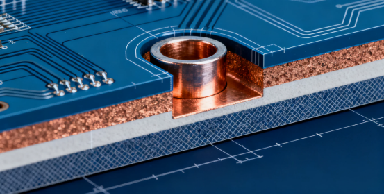
Imagine a high-rise building with only staircases and no elevators—people movement efficiency would be severely compromised. Plated through-holes in PCBs function like “elevators,” transmitting signals and power across different circuit layers.
Unlike surface copper thickness, hole copper thickness is entirely determined by the electroplating process. After each drilled hole is created, the electroplating process is used to deposit copper onto the hole wall of the drilled hole. Copper is electroplated onto the inner walls to ensure electrical connectivity and mechanical strength. The fluidity, concentration of the plating solution, and process parameters all influence the final product’s uniformity and thickness.
Why is 25μm the "Safety Threshold" for Hole Copper Thickness?

The Physics of Current Carrying Capacity
According to the formula R = ρL/A (Resistance = Resistivity × Length / Cross-sectional Area), when current passes through a plated through-hole, copper thickness directly determines resistance value. Thinner copper layers mean higher resistance and greater heat generation.
Copper weight is another important parameter, as it influences both the current-carrying capacity and the required trace width for reliable PCB performance.
The 25μm value isn’t arbitrarily set but represents a balance point derived from extensive experimentation and field data:
·When hole copper thickness falls below 20μm, resistance increases significantly
·At 25μm, resistance reaches a relatively ideal balance point
·Further thickness increases yield diminishing returns while costs rise substantially
The Brutal Test of Thermal Stress
PCBs undergo severe temperature challenges during assembly and operation:
·Reflow soldering process: Temperature rises to 260°C within minutes
·Ambient temperature fluctuations: Extreme variations from -40°C to +125°C
·Self-heating effects: Temperature rise during high-current operation
Different materials exhibit vastly different thermal expansion coefficients:
·FR-4 substrate: CTE approximately 14-18 ppm/°C (XY direction)
·Copper material: CTE approximately 17 ppm/°C
During temperature changes, the substrate and copper expand and contract at different rates. Sufficient copper thickness resists this stress, preventing microcracks in the hole walls. The inner layers of the PCB are also affected by thermal stress, so ensuring adequate copper thickness in these inner layers is crucial for long-term reliability.
Base Copper Thickness and Its Effects
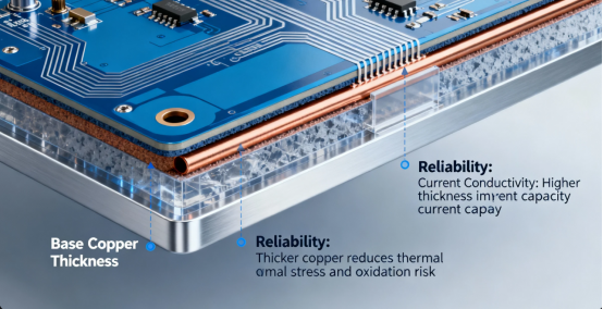
When designing a printed circuit board, the journey to reliable electrical connections and robust mechanical strength begins with the base copper thickness. This parameter refers to the initial copper layer applied to the PCB substrate before any additional plating or processing takes place. In the pcb manufacturing process, the base copper thickness forms the foundation upon which all subsequent copper layers and hole plating are built.
Typically measured in ounces per square foot (oz), with 1 oz being a common industry standard, the base copper thickness directly influences the finished copper thickness—the total copper present after all plating steps are complete. This finished copper thickness is crucial, as it determines not only the trace width and current-carrying capacity on the surface but also the final hole copper thickness within plated through-holes.
A thicker base copper layer can enhance the electrical conductivity and thermal stability of the circuit board, providing a stronger backbone for both traces and pcb holes. This is especially important in applications demanding higher reliability, where the final hole copper must withstand thermal cycling and mechanical stress. However, increasing the base copper thickness also raises material costs and can complicate the manufacturing process, particularly when fine features or multiple layers are involved.
Manufacturers like PCBWay offer a range of base copper thickness options to accommodate different design requirements, from thin copper for high-density, low-power boards to heavy copper for power electronics and industrial applications. By carefully specifying the base copper thickness during the design phase, engineers can ensure that the finished copper thickness—including the critical hole copper thickness—meets the necessary standards for performance and reliability.
Ultimately, controlling the base copper thickness is a key step in achieving the desired final hole copper and ensuring the long-term quality of the printed circuit board. It’s a foundational decision that impacts every layer, every hole, and every electrical connection on the board.
Hole Size and Shape Considerations
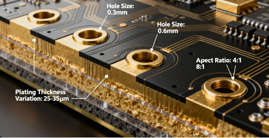
The dimensions and geometry of pcb holes are far more than a matter of simple preference—they are pivotal factors that directly affect hole copper thickness, manufacturing complexity, and the overall reliability of the circuit board. In the pcb manufacturing process, both the size and shape of each hole must be carefully engineered to ensure robust electrical connections and mechanical integrity.
Larger holes, for example, require more copper plating to achieve the specified hole copper thickness. This not only increases material usage and process time but can also drive up manufacturing costs. Conversely, smaller holes—while beneficial for high-frequency signal performance and enabling more compact designs—pose their own challenges. Achieving uniform copper thickness in small-diameter holes, especially when the board itself is thick, demands precise control over the plating process.
A critical metric here is the aspect ratio, defined as the ratio of the board thickness to the hole diameter. Higher aspect ratios mean deeper, narrower holes, which are more difficult to plate evenly with copper. As the aspect ratio increases, ensuring adequate hole copper thickness becomes more challenging, potentially impacting the reliability of electrical connections and the board’s ability to withstand thermal and mechanical stress.
The drilling process also plays a significant role. Different drilling methods—mechanical, laser, or micro-drilling—offer varying levels of accuracy and can influence the final hole shape and size. Any deviation can affect the uniformity of the copper layer deposited during plating, further impacting the final hole copper.
In advanced designs, such as high-density interconnect (HDI) PCBs, the use of smaller holes and microvias allows for greater component density and more complex routing. However, these benefits come with the need for advanced manufacturing techniques to maintain the required copper thickness and ensure long-term reliability.
Ultimately, careful consideration of hole size and shape during the design phase is essential. By understanding the interplay between these factors and the copper plating process, designers can optimize for both performance and manufacturability, ensuring that every hole—regardless of size or shape—meets the stringent requirements for electrical and mechanical reliability in modern circuit boards.
Which Applications Must Adhere to the 25μm Standard?
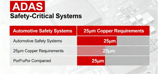
1. Automotive Electronics: No Compromise on Safety
Electronic control systems in modern vehicles directly impact safety:
·Engine Control Units (ECUs): Must withstand operating temperatures from -40°C to +125°C
·Brake control systems: Any signal interruption could cause catastrophic consequences
·Airbag controllers: Must maintain absolute reliability throughout the vehicle’s lifespan
Failure analysis reports from a renowned automotive manufacturer reveal that 93% of failures related to hole copper issues directly correlate with thickness below 20μm.
Automotive PCBs are manufactured under stringent quality controls to ensure compliance with hole copper thickness standards.
2. Industrial Equipment: Ensuring Continuous Stable Operation
Industrial environments impose extreme demands on electronic devices:
·Motor drive systems: Continuous high-current operation
·Process control systems: Require 24/7 uninterrupted operation
·Industrial robots: Frequent vibration and mechanical stress
Industrial equipment typically targets 10-15 years of expected lifespan, far exceeding the 3-5 years for consumer electronics. Thicker hole copper ensures connection reliability after prolonged use.
Unless specific requirements are provided, manufacturers generally assume standard tolerances for hole copper thickness in industrial applications.
3. Aerospace: Survival in Extreme Environments
Aerospace applications push reliability requirements to the extreme:
·Temperature extremes: From -55°C at high altitudes to +85°C in direct sunlight
·Pressure variations: Frequent pressure differential cycles
·Vibration environments: Continuous mechanical vibration
In these applications, 25μm represents the minimum requirement, with many scenarios demanding 30μm or higher. Industry standards, such as IPC-4562, also specify the maximum allowable reduction in copper thickness—typically permitting up to a 10% decrease from the nominal value—to ensure consistent reliability.
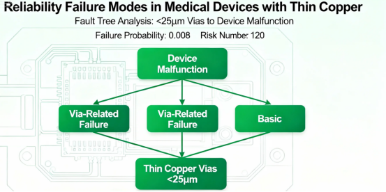
4. Medical Devices: Foundation of Life Support
Medical electronic devices inherently demand exceptional reliability:
·Life-sustaining equipment: Any failure could endanger lives
·Implantable devices: No possibility for on-site repairs
·Diagnostic equipment: Reliability directly affects diagnostic outcomes
For these applications, a 25μm or higher hole copper thickness is the preferred standard for medical device PCBs.
Potential Risks of Insufficient Hole Copper Below 25μm
Case 1: New Energy Vehicle Charging Module Failure
A charging station manufacturer discovered 3% of products failed during warranty after mass production. Root cause analysis revealed plated through-hole copper thickness of only 18μm. During high-current (30A) operation, local temperatures exceeded 150°C, causing microcracks in hole walls that eventually led to complete disconnection. Such failures often become apparent only at a later stage, such as during field operation or warranty analysis.
Case 2: Seasonal Failures in Industrial Controllers
A PLC manufacturer observed significantly higher failure rates for outdoor-installed controllers during winter. Investigation revealed that when temperatures dropped below -20°C, boards with thinner hole copper (16μm) experienced intermittent connection failures. The problem resolved completely after increasing thickness to 25μm.
Case 3: Signal Degradation in Communication Base Stations
5G base station equipment exhibited signal quality degradation after one year of operation. Analysis showed uneven hole copper thickness (15-22μm) caused impedance deviations, affecting high-frequency signal integrity. Signal stability improved significantly after standardizing to 25μm.
Using higher copper weights, such as 1 oz. or 2 oz., can further help maintain signal integrity in high-frequency applications by providing more consistent trace performance and reducing impedance variations.
How to Ensure Hole Copper Thickness Meets Standards?

Design Phase Considerations
Clear Specification Requirements
·Explicitly mark "Hole Copper Thickness ≥25μm" in Gerber files and fabrication notes
·Reference relevant IPC standards (IPC-6012 Class 3)
Rational Via Design
·Control aspect ratio (board thickness/hole diameter) within 8:1
·Use multiple parallel vias for high-current paths
Manufacturing Process Selection
Supplier Evaluation
·Select manufacturers with appropriate process capabilities
·Request hole copper cross-section reports and quality data
Process Control
·Precise control of plating solution composition and concentration
·Appropriate current density and plating time
·Regular process parameter verification
The initial copper foil thickness is a key parameter in determining the final hole copper thickness, as it sets the baseline for copper build-up according to IPC-A-600J-Class 2 standards.
Quality Verification Methods
Destructive Testing
·Microsection analysis: Most direct thickness measurement method
·Thermal stress testing: Evaluates hole copper durability
Non-Destructive Testing
·Four-wire low-resistance testing: Indirectly assesses hole copper quality
·Automated optical inspection: Monitors surface uniformity
Balancing Cost and Reliability

Choosing 25μm hole copper thickness does increase costs, primarily in:
·Material costs: Higher copper consumption
·Process costs: Longer plating times and stricter process control
·Inspection costs: More comprehensive quality verification
However, compared to potential risks, these cost investments are necessary:
·Field failure repair costs typically range from 10-100 times prevention costs
·Brand reputation damage is difficult to quantify financially
·Liability risks in safety-related applications could threaten business survival
Conclusion
In PCB design and manufacturing, 25μm hole copper thickness isn't an arbitrarily chosen value but a reliability threshold determined based on physical principles, extensive experimental data, and field experience.
For products that must operate reliably in extreme environments, carry high currents, or involve safety-critical applications, 25μm isn't a "recommendation" but a "necessity". This additional 5μm of thickness provides products with extra safety margin against thermal stress, mechanical stress, and electrical strain.
Next time you design a PCB, remember: appropriate investment in hole copper thickness constitutes an "insurance policy" for long-term product reliability. In reliability-critical applications, insisting on 25μm hole copper thickness isn't a cost but an investment—a commitment to product quality and responsibility toward end-users.
FAQs
Q.Why is there a requirement for PCB hole copper thickness to exceed 25 microns?
A.To ensure reliable electrical conductivity, meet current-carrying capacity needs, and enhance the mechanical strength and corrosion resistance of the holes, preventing issues like poor contact or hole wall damage during use.
Q.In which applications is this requirement particularly critical?
A.High-power electronics (e.g., power supplies), automotive electronics, aerospace equipment, and industrial control systems. These scenarios have higher demands for current transmission and product durability.
Q.What problems may arise if the copper thickness is less than 25 microns?
A.Insufficient current-carrying capacity leading to overheating, increased signal loss, poor adhesion between the copper layer and the hole wall, and reduced resistance to thermal cycling and corrosion, which shortens the PCB's service life.
Q.How is the hole copper thickness typically measured and controlled during manufacturing?
A.Commonly measured using a microsection analyzer. Controlled by optimizing electroplating parameters (current density, time, temperature) and adopting high-quality electroplating solutions to ensure uniform and sufficient copper layer deposition.
Q.Does the 25-micron requirement apply to all PCBs?
A.No. For low-power, low-reliability demand products (e.g., ordinary consumer electronics accessories), lower hole copper thickness (e.g., 18-20 microns) may be acceptable, depending on specific design requirements.
Author: Jack Wang

