


2 Layer Printed Circuit Board: What It Is, Features, and Applications
Printed circuit boards are the foundation of almost every electronic device, quietly connecting components and enabling complex circuits to function. Among them, the 2 layer printed circuit board offers an ideal combination of simplicity, reliability, and versatility. From small DIY projects to everyday consumer electronics, its design makes it a practical choice for many applications. Understanding what makes a 2 layer PCB distinct and how it is used can provide valuable insights for anyone interested in electronics design.
Introduction to 2 Layer Printed Circuit Boards
Definition of a 2 Layer PCB
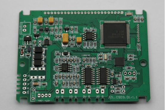
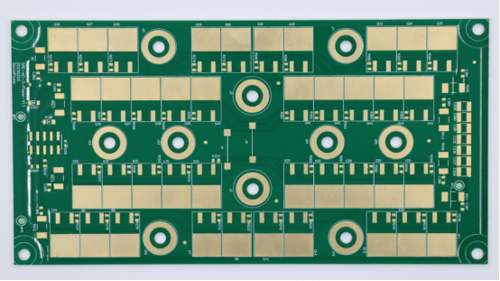
A 2 layer printed circuit board (PCB) is a type of PCB that contains two conductive copper layers separated by an insulating material, usually a substrate such as FR-4. One layer typically carries signal traces, while the other often serves as a ground or power plane, allowing circuits to be more compact and organized compared to single-layer PCBs.
In simple terms, imagine a sandwich: the copper layers are the “bread,” and the insulating substrate is the “filling” that keeps them apart. This structure allows designers to route signals on multiple layers without short circuits.
Example: A small microcontroller project might use a 2 layer PCB where the top layer handles component connections and signal paths, while the bottom layer provides a continuous ground plane for stability and reduced electrical noise.
Brief History and Evolution
The concept of 2 layer PCBs emerged as electronic devices became more complex in the mid-20th century. Early electronics relied mostly on single-layer boards, which were simpler but limited in routing capacity. As circuits demanded more connections, the 2 layer PCB allowed for denser layouts without increasing board size.
Over time, PCB manufacturing technologies advanced. Techniques such as photolithography, precise etching, and automated drilling enabled consistent production of 2 layer boards at higher volumes and lower costs. These improvements also made it possible to achieve smaller trace widths and tighter spacing, supporting modern electronic devices.
Importance in Modern Electronics
2 layer PCBs remain widely used because they strike a balance between simplicity and functionality. They are ideal for low-to-mid complexity devices, where a single layer is insufficient but a multilayer board is unnecessary.
Examples of common applications:
Consumer electronics: remote controls, LED lighting circuits, small gadgets.
Industrial devices: simple sensor boards or controllers.
Educational projects: microcontroller kits and DIY electronics.
The design of 2 layer PCBs allows for efficient signal routing, reduced electrical noise, and compact layouts, making them cost-effective and reliable.
Comparison with Other PCB Layer Counts
Single-Layer PCB vs 2 Layer PCB
A single-layer PCB contains only one conductive copper layer, typically used for simple circuits with minimal connections. In contrast, a 2 layer PCB has two conductive layers separated by an insulating substrate, allowing more complex signal routing and component placement.
Key differences:
Signal routing: 2 layer PCBs enable more sophisticated layouts, reducing the need for jumpers or wiring bridges. Single-layer boards are limited to straightforward connections.
Cost: Single-layer PCBs are generally cheaper to produce, making them ideal for low-cost devices. 2 layer PCBs are slightly more expensive due to additional materials and manufacturing steps.
Typical applications: Single-layer PCBs are common in toys, basic calculators, or LED projects. 2 layer PCBs are often found in mid-range consumer electronics, microcontroller boards, and small industrial devices.
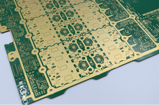
2 Layer PCB vs Multi-Layer PCB
Multi-layer PCBs contain three or more conductive layers, designed for high-density circuits and advanced electronics requiring compact layouts. While they allow intricate routing and additional power/ground planes, multi-layer PCBs are more difficult and expensive to manufacture.
Key differences:
Complexity: Multi-layer boards support high-density circuits for advanced devices like smartphones, servers, or communication equipment. 2 layer PCBs are simpler and sufficient for low-to-mid complexity electronics.
Manufacturing and maintenance: 2 layer PCBs are easier to fabricate, assemble, and repair. Multi-layer PCBs require precise manufacturing processes and are more challenging to troubleshoot.
Cost-effectiveness: 2 layer PCBs offer a good balance between functionality and affordability, while multi-layer PCBs are significantly more costly.
Visual Comparison Table
Layer Count
Complexity
Cost
Typical Applications
1 Layer
Simple circuits
Low
Toys, calculators, LED projects
2 Layers
Moderate complexity
Medium
Microcontroller boards, consumer electronics, small industrial devices
3+ Layers
High-density circuits
High
Smartphones, servers, communication devices
Layer Count
Complexity
Cost
Typical Applications
1 Layer
Simple circuits
Low
Toys, calculators, LED projects
2 Layers
Moderate complexity
Medium
Microcontroller boards, consumer electronics, small industrial devices
3+ Layers
High-density circuits
High
Smartphones, servers, communication devices
Structure and Design of 2 Layer PCBs
Basic Components and Materials
A typical 2 layer PCB consists of several essential components and materials:
Copper layers: Two conductive layers that carry electrical signals and power.
Substrate materials: Common options include FR-4, a glass-reinforced epoxy, and CEM-1, a paper-epoxy composite. These substrates provide insulation and mechanical support.
Solder mask: A protective layer applied over copper traces to prevent oxidation and short circuits.
Silkscreen: Printed markings used to indicate component placement and reference designators.
Material differences:
Durability: FR-4 is stronger and more heat-resistant than CEM-1.
Cost: CEM-1 is cheaper but less robust, suitable for low-cost projects.
Performance: FR-4 supports higher-frequency signals and better long-term reliability.
Example: A small LED controller might use CEM-1 for cost savings, while a microcontroller board for industrial use would prefer FR-4 for reliability.
Layer Configuration and Layout
In a 2 layer PCB, the two copper layers are usually assigned specific roles:
Top layer: Often used for signal traces and component placement.
Bottom layer: Typically serves as a ground or power plane, reducing electrical noise and improving signal stability.
Design considerations for trace routing:
1. Plan signal paths to minimize crossing and interference.
2. Keep traces as short and direct as possible to reduce resistance and inductance.
3. Use vias to connect traces between layers efficiently.
Step-by-step example:
1. Place components on the top layer according to functionality.
2. Route critical signal traces on the top layer first.
3. Use the bottom layer for ground connections and less critical signals.
4. Review trace spacing and width to meet electrical and manufacturing standards.
Design Considerations for Beginners
For those new to PCB design, the following best practices can improve functionality and manufacturability:
Minimum trace width and spacing: Follow manufacturer specifications, commonly 6–8 mils for moderate-density boards.
Component placement: Place high-speed or sensitive components close to related circuitry to maintain signal integrity.
Ground continuity: Ensure the bottom layer provides a continuous ground plane where possible.
Avoid sharp angles: Use 45° angles instead of 90° in traces to reduce signal reflections.
Example: When designing a simple microcontroller board, place power input, microcontroller, and critical sensors near each other on the top layer, route signal traces efficiently, and use the bottom layer for a solid ground plane.
Key Features of 2 Layer PCBs
Electrical Characteristics
2 layer PCBs provide important electrical advantages for medium-complexity circuits.
Signal routing: The two layers allow designers to route more traces without overlap, reducing the need for jumpers or complicated wiring.
Current capacity: Copper thickness and trace width determine how much current a board can safely carry. Standard 2 layer boards handle typical small-to-medium electronic device currents efficiently.
Potential crosstalk: By separating signal and ground layers, 2 layer PCBs reduce electromagnetic interference and signal degradation, though not as effectively as multi-layer boards.
Example: In a microcontroller project, sensitive analog signals can be routed on one layer while power and ground connections occupy the other, minimizing interference.
Mechanical Properties
The mechanical design of 2 layer PCBs ensures durability and stability for a wide range of applications:
Rigidity: The substrate material (e.g., FR-4) provides stiffness to support components.
Thickness: Typical boards range from 1.0 to 1.6 mm, balancing flexibility and strength.
Durability: 2 layer PCBs withstand moderate thermal stress and mechanical handling, making them suitable for consumer electronics, industrial devices, and prototypes.
Example: A 2 layer LED driver board uses FR-4 material to provide enough stiffness for repeated handling without bending or cracking.
Advantages and Limitations
Advantages:
Cost-effective: Cheaper to manufacture than multi-layer PCBs, making them ideal for low-to-mid-range products.
Widely available: Supported by most PCB manufacturers.
Easy to manufacture and repair: Less complex than multi-layer boards, simplifying assembly and troubleshooting.
Limitations:
Limited space: Only two layers for routing traces, which restricts highly complex circuits.
Crosstalk potential: More prone to electromagnetic interference compared to multi-layer PCBs for high-speed signals.
Comparison Table:
Feature | Single-Layer PCB | 2 Layer PCB | Multi-Layer PCB |
|---|---|---|---|
Complexity | Simple circuits | Moderate complexity | High-density circuits |
Cost | Low | Medium | High |
Manufacturability | Easy | Moderate | Complex |
Signal Routing | Limited | More flexible | Highly flexible |
Typical Applications | Toys, LEDs | Microcontrollers, consumer electronics | Smartphones, servers, communication devices |
Applications of 2 Layer PCBs
Consumer Electronics
2 layer PCBs are widely used in consumer electronic devices due to their cost-effectiveness and moderate complexity. They allow designers to implement reliable circuits without the need for expensive multi-layer boards.
Examples include:
Smartphones: Small interface boards or accessory circuits.
Keyboards and mice: Connection and signal routing boards.
LED devices: Lighting controllers and simple display modules.
Example: An LED desk lamp may use a 2 layer PCB to connect the power supply, LEDs, and control switch efficiently without excess cost.
Industrial and Automotive Electronics
In industrial and automotive applications, 2 layer PCBs are valued for their mechanical stability and reliability under moderate environmental stress. They are often deployed where high-density circuits are unnecessary, but durability is important.
Examples include:
Control boards: Used in machinery or factory automation for medium-complexity circuits.
Automotive dashboards: Signal and power distribution boards for basic features like lighting or sensors.
Benefits in rugged environments:
The substrate material (e.g., FR-4) provides stiffness and thermal resistance.
Suitable for moderate vibration and temperature ranges.
Easier to repair compared to multi-layer boards.
Example: A factory sensor controller may use a 2 layer PCB to connect input/output modules, ensuring reliable operation while keeping manufacturing costs manageable.
Prototyping and Educational Use
2 layer PCBs are ideal for learning, testing, and proof-of-concept projects because they balance simplicity with practical circuit design. Beginners and educators can experiment with real circuits without the complexity of multi-layer boards.
Example:
Building a basic LED circuit on a 2 layer PCB:
1. Place LEDs and resistors on the top layer.
2. Route signal traces carefully to minimize crossings.
3. Use the bottom layer as a ground plane.
4. Test the circuit for functionality before moving to more complex designs.
Manufacturing and Assembly Process
PCB Fabrication Steps
The fabrication of a 2 layer PCB involves several key steps that transform raw materials into a functional circuit board:
1. Substrate preparation: The insulating substrate, typically FR-4, is cleaned and prepped to ensure smooth copper adhesion.
2. Copper layering: Both sides of the substrate are laminated with copper foil.
3. Etching: Unnecessary copper is removed using chemical etchants, leaving only the desired circuit traces.
4. Drilling: Holes for vias and through-hole components are drilled precisely.
5. Plating: Copper is plated in drilled holes to create reliable electrical connections between layers.
Example: A microcontroller development board undergoes these steps to create a compact 2 layer design that connects all input/output components reliably.
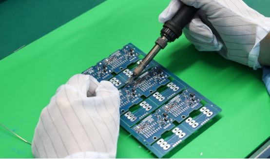
Soldering and Component Assembly
Once the PCB is fabricated, components are mounted and soldered using one of two methods:
Through-hole technology (THT): Component leads pass through holes in the PCB and are soldered on the opposite side. Ideal for mechanical stability.
Surface-mount technology (SMT): Components are soldered directly onto pads on the surface of the PCB. Enables compact layouts and is widely used in modern electronics.
Tips for beginners:
Verify component orientation before soldering to avoid malfunction.
Avoid overheating solder joints, which can damage the PCB.
Use flux sparingly to prevent residue that may affect conductivity.
Example: A 2 layer LED controller may use SMT for small resistors and LEDs while using THT for a robust power switch.
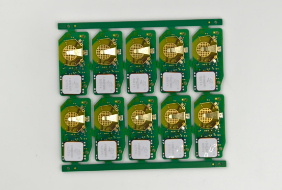
Quality Testing and Inspection
After assembly, quality control ensures reliability and proper functioning:
Visual inspection: Check for solder bridges, missing components, and alignment issues.
Electrical testing: Continuity tests and functional testing verify that signals and power paths work correctly.
Reliability checks: Thermal cycling and mechanical stress tests confirm durability for intended applications.
Example: Before shipping, a microcontroller prototype board undergoes continuity tests and a heat stress check to guarantee it performs correctly in real-world conditions.
Future Trends and Innovations
Technological Improvements
2 layer PCBs continue to evolve with advancements in materials and design techniques.
New substrate materials: Manufacturers are exploring advanced polymers and composites that offer higher thermal resistance, lower signal loss, and improved mechanical strength compared to traditional FR-4.
Higher trace precision: Modern fabrication techniques allow narrower traces and smaller spacing, enabling more compact circuits even on just two layers.
Hybrid designs: Some 2 layer PCBs integrate embedded components or partial multi-layer structures to combine the simplicity of two layers with certain benefits of multi-layer boards.
Example: A compact IoT sensor module may use a 2 layer PCB with high-precision traces and a hybrid layout to fit all components in a small form factor while maintaining reliable signal performance.
Sustainability and Cost Efficiency
Modern PCB design is increasingly focused on reducing environmental impact and production costs.
Eco-friendly materials: Substrates made from recycled or low-toxicity components reduce environmental footprint.
Recycling strategies: End-of-life boards can be dismantled to recover copper and other valuable materials.
Cost reduction strategies: Optimized layouts, standardized components, and efficient manufacturing techniques help keep 2 layer PCB production affordable.
Example: An educational electronics kit may use 2 layer PCBs made from partially recycled FR-4, minimizing both cost and environmental impact while maintaining board performance.
Conclusion
In today’s electronics landscape, 2 layer PCBs remain a versatile and cost-effective choice for a wide range of applications—from consumer gadgets to industrial and educational projects. Their balance of simplicity, reliability, and manufacturability makes them an essential component for designers at any level. For companies and engineers seeking expert support in designing and manufacturing high-quality 2 layer PCBs, PCBMASTER offers decades of experience, advanced technology, and a commitment to delivering reliable solutions tailored to every project’s needs.
FAQs
1. What is the difference between a 2 layer PCB and a multilayer PCB?
2 Layer PCB: Contains two conductive copper layers separated by an insulating substrate. It is suitable for low-to-medium complexity circuits, cost-effective, and easier to manufacture and repair.
Multilayer PCB: Contains three or more conductive layers. It supports high-density and complex circuits, allows additional power/ground planes, and is commonly used in advanced electronics like smartphones and servers. Multilayer PCBs are more expensive and require precise manufacturing.
2. Can beginners design and manufacture their own 2 layer PCB?
Yes, beginners can design and produce 2 layer PCBs. They can use PCB design software (like KiCad or Eagle) to plan the layout, ensuring proper trace spacing and component placement. Many PCB manufacturers and DIY kits support small batch production of 2 layer boards, making prototyping accessible.
3. How does a 2 layer PCB affect electronic device performance?
2 layer PCBs allow better signal routing compared to single-layer boards, reducing wiring complexity and improving reliability. The separate layers for signals and ground help minimize crosstalk and electromagnetic interference, which supports stable device performance. However, they have limited space for very high-density circuits compared to multilayer PCBs.
4. What are the most common mistakes when designing a 2 layer PCB?
Placing components too close together, causing routing difficulties or thermal issues.
Using traces that are too thin for the intended current, risking overheating.
Ignoring ground plane continuity, which can increase noise and signal interference.
Sharp 90° trace angles, which can cause signal reflections.
Failing to check component orientation before assembly, leading to malfunction.
5. How long do 2 layer PCBs typically last in industrial applications?
The lifespan depends on material quality, operating conditions, and thermal/mechanical stress. Typical FR-4 2 layer PCBs can last 10–20 years in standard industrial environments if properly designed and maintained. High-temperature or high-vibration conditions may reduce lifespan, while protective coatings and careful design can extend it.

