


Transparent Glass PCB The Invisible Circuit Changing How We Design Gadgets
Introduction
If you’ve ever looked at a smartphone screen, a smartwatch display, or a digital sign, you’ve probably noticed something: the electronics powering those screens are almost always hidden. The green PCB (printed circuit board) with its copper lines is tucked away behind the display, out of sight. But what if the PCB itself could be transparent—so it blends right into the screen, turning your device into a seamless, all-glass panel?
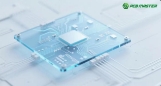
That’s exactly what transparent glass PCBs do—they are a new type of printed circuit boards designed to be nearly invisible while still providing full electronic functionality. The pcb industry is being transformed by the introduction of transparent substrates like glass, which enable new design possibilities and applications in high-tech devices.
Unlike traditional PCBs made of FR-4 (the green, fiberglass-based material you’re used to), transparent glass PCBs use ultra-thin, clear glass as their base. Transparent substrates such as glass are chosen for their unique properties. Instead of thick copper traces, they rely on see-through conductive materials (like indium tin oxide, or ITO) to carry electricity. The result? A circuit board that’s nearly invisible—you can see right through it while it powers your device. According to the glass pcb material specification, ultra-clear float glass is used as the primary substrate, offering high thermal conductivity, excellent electrical insulation, and strong mechanical strength.
In this guide, we’ll break down everything you need to know about transparent glass PCBs: what they are, how they work, why they’re a game-changer for design, and where you’ll start seeing them (spoiler: they’re already in some of your favorite gadgets). No engineering degree required—just a curiosity about the future of electronics.
First: Why Do We Need Transparent Glass PCBs?
Traditional FR-4 PCBs are great—they’re cheap, durable, and work for most devices. But they have a big limitation: they’re opaque. That means if you want to build a device where the electronics need to be seen (or not seen), FR-4 fails.
Transparent glass PCBs are a specialized type of printed circuit designed for high-performance and aesthetic applications, offering unique benefits over traditional substrates.
Let’s think about real-world problems transparent glass PCBs solve:
Glass is widely used in electronics and optoelectronics, where its transparency, electrical insulation, and thermal stability are crucial. Transparent PCBs made from glass enable innovative designs in display technologies, LED lighting, and advanced sensors, supporting applications that require both visibility and high performance.
The advantages of glass include excellent impact resistance, high-temperature resistance, low thermal expansion, and suitability for high-frequency and high-speed electronic applications such as RF circuits and 5G technology. These properties make glass PCBs ideal for advanced electronic devices that demand durability and superior performance.
Seamless Displays (No More "Bezels")
Ever wished your smartphone or laptop screen didn’t have that thick black border (called a “bezel”) around it? Those bezels exist partly because the PCB powering the screen has to fit around the edges—since it’s green and opaque, it can’t be under the display itself. Transparent PCBs, including transparent glass PCBs, are now used in advanced display technologies, allowing circuit boards to be placed directly beneath the screen without being visible.
Transparent glass PCBs change that. Since they’re clear, they can be placed directly under the screen. This lets manufacturers shrink bezels to almost nothing, creating “all-screen” devices. Using a transparent PCB enables the creation of devices with minimal bezels and seamless displays. Imagine a laptop where the entire lid is a display, or a smart mirror that doesn’t have a clunky circuit board hiding behind it—transparent glass PCBs make that possible.
"Invisible" Electronics for Aesthetics
Designers love transparent glass PCBs because they let electronics blend into their surroundings. Think about:
·Smart home devices: A wall-mounted thermostat that looks like a piece of glass, not a gadget with a hidden PCB. Using a see through circuit board helps achieve this minimalist, invisible look.
·Wearables: A smartwatch where the circuit board doesn’t block the display—so the watch face feels like a single, smooth piece.
·Art installations: Digital art that uses transparent circuits to power LEDs, making the art itself the focus, not the electronics.
Better Performance for High-Tech Screens
Glass isn’t just clear—it’s also heat-resistant and stable. Glass PCBs have superior thermal characteristics compared to traditional FR-4 PCBs, including high thermal conductivity and excellent thermal conductivity, which enable efficient heat dissipation. Traditional FR-4 PCBs can warp or overheat when used with high-brightness screens (like OLED or Mini LED displays). The high thermal conductivity of glass PCBs allows them to maintain performance and durability in demanding applications, making them ideal for devices that need bright, long-lasting displays (think: digital billboards, medical monitors, or car infotainment systems).
Flexible (Yes, Even Glass!)
You might think glass is brittle, but transparent glass PCBs use ultra-thin glass (sometimes as thin as 0.1mm—thinner than a human hair). This glass is flexible enough to bend slightly, making it perfect for foldable devices. Flexible transparent PCBs, made with ultra-thin glass or flexible substrates like PET film and polyimide, enable innovative device designs such as wearable tech, curved displays, and compact, lightweight electronics. Flexible circuits can also be achieved using ultra-thin glass substrates, expanding the possibilities for wearable and foldable electronics. Imagine a foldable phone where the PCB bends with the screen, no creaks or cracks—transparent glass PCBs make that safer and more reliable.
What Is a Transparent Glass PCB, Exactly?
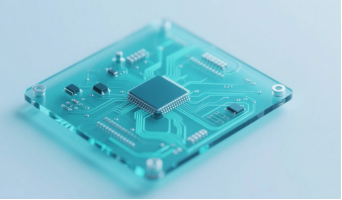
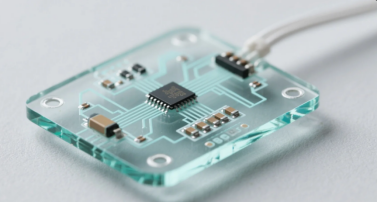
Let’s start with the basics: A transparent glass PCB is a type of glass printed circuit board where two key parts are clear:
·The Base (Substrate): Instead of FR-4, the “backbone” or substrate material of the PCB is a sheet of ultra-thin, high-quality glass. Using glass substrates offers advantages such as excellent electrical insulation, thermal stability, and mechanical strength, making them ideal for high-performance applications. This glass is usually made of soda-lime glass (like the glass in your phone screen) or borosilicate glass (more heat-resistant, used in medical devices). Glass fibers and other insulating material may be incorporated to further enhance mechanical and electrical properties. It’s clear, smooth, and strong enough to support electronic components.
·The Conductive Traces: Instead of copper (which is opaque), the lines that carry electricity are made of transparent conductive materials. The most common one is ITO (Indium Tin Oxide), a thin film that’s both see-through and a good conductor of electricity. Other options include FTO (Fluorine-Doped Tin Oxide) or even ultra-thin silver nanowires (which are almost invisible). In some glass PCBs, a metal layer or copper foil may be used for specific high-conductivity or high-power applications.
Epoxy resin can also be used as an insulating layer within the structure, providing additional durability and thermal stability. Compared to other types of glass PCBs, such as glass copper pcb, transparent glass PCBs use see-through conductive materials rather than traditional copper, offering unique optical and design advantages.
The rest of the PCB works like a traditional one: it has soldered components (like resistors, capacitors, or chips), and it connects to other parts of the device. The difference? You can see through the board itself—so the only things you notice are the small components, not the circuit lines.
Transparent glass PCBs are part of a broader family of advanced circuit boards that utilize innovative materials and structures for specialized applications.
How Are Transparent Glass PCBs Made? (The Simplified Version)
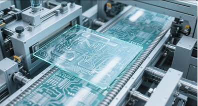
Making a transparent glass PCB is more complex than making a traditional FR-4 PCB, but the process boils down to 5 key steps. In traditional pcb manufacturing, a copper board is used as the base material, where photoresist is applied, exposed, and etched to form circuit pathways. In contrast, transparent glass PCBs use a glass substrate and require specialized techniques such as UV curing and etching. Mass production methods are being developed to make these innovative transparent glass PCBs more widely available. Let’s break it down like you’re watching a factory tour:
Step 1: Choose the Right Glass Substrate
First, manufacturers pick a glass substrate. The glass needs to be:
·Ultra-thin: Usually 0.1mm to 0.5mm thick (thicker glass is less flexible and harder to integrate into small devices).
·Clear: No bubbles or scratches—even tiny flaws would show through in the final device.
·Smooth: The surface has to be perfectly flat so the conductive material (like ITO) sticks evenly.
For applications that require enhanced durability and impact resistance, tempered glass is often selected due to its strength, thermal properties, and suitability for high-stress environments.
Most factories use glass from companies like Corning (the same company that makes Gorilla Glass for phone screens) because it’s durable and consistent.
Step 2: Add the Transparent Conductive Layer
Next, the glass gets a thin coating of ITO (or another transparent conductor). This is done using a process called sputtering:
·The glass is placed in a vacuum chamber.
·ITO is heated until it turns into a vapor.
·The vapor sticks to the glass, forming a thin, even film (usually just 50-100 nanometers thick—1/1000 the thickness of a human hair).
This ITO film acts as the metal layer responsible for electrical conductivity in the transparent glass PCB.
This ITO layer is what will become the “traces” (the lines that carry electricity) on the PCB.
Step 3: Etch the Circuit Pattern
Now, the ITO layer needs to be shaped into the right circuit pattern (the lines that connect components). This uses a process called photolithography—similar to how computer chips are made:
·The ITO-coated glass is carefully covered with a photo resist or UV-sensitive resist film. It's important to avoid air bubbles during this step for proper adhesion. Sometimes, scotch tape is used to help handle the resist film or remove its protective cover layer.
·The circuit pattern is first printed onto a transparent sheet, which is then used to create an opaque film mask. This opaque film blocks UV light in areas where you don't want the resist to cure.
·The opaque film is placed over the glass, and a UV curable mask (or uv curable masks) is applied. The setup is then exposed to UV light using a uv light source or artificial uv source. Bright sunlight can also be used as an alternative for exposure, but the setup must remain stable during this process. The UV light hardens the photo resist or uv resist films in the areas where the circuit lines will be.
·After exposure, the glass is developed by immersing it in a baking soda solution (a low basic solution) to remove the uncured resist. Rinse powder can be used as an alternative developer if baking soda is unavailable. This step reveals only the tracks and pads needed for the circuit. The pads layer should be isolated and exported from the layer pallet to ensure only the tracks and pads are included in the layout.
·The developed, cured resist tracks now protect the desired circuit areas. The glass is then placed in a ferric chloride solution to etch away unwanted copper or ITO, leaving behind only the intended circuit pattern.
·Finally, the remaining resist is stripped off, resulting in a glass sheet with invisible circuit lines—you can see right through them, but they’re ready to carry electricity.
Step 4: Solder the Components
Next, small electronic components (like chips, resistors, or LEDs) are soldered onto the ITO traces. This is trickier than soldering to copper: ITO is more fragile, so manufacturers use low-temperature solder (to avoid damaging the glass) and tiny, lightweight components (since heavy parts could crack the thin glass). To protect the ITO traces during and after soldering while maintaining the transparency of the PCB, a clear solder mask is often applied.
Some factories use robots for this step—they’re more precise than human hands, which is crucial for small, delicate circuits.
Step 5: Test and Finish
Finally, the transparent glass PCB is tested to make sure it works:
·Engineers check if electricity flows correctly through the ITO traces.
·They test the PCB’s durability (can it bend slightly without breaking? Does it handle heat well?).
·They add a thin protective coating (like a clear polymer) to prevent scratches or damage to the ITO layer.
If everything passes, the PCB is ready to be integrated into a device—like a smartphone screen or a smart mirror.
Designing Circuits for Transparent Glass PCBs: New Rules for the Invisible
Designing circuits for transparent glass PCBs isn’t just about making things look cool—it’s about rethinking the rules of circuit design from the ground up. When your printed circuit board is see-through, every detail matters, from the choice of materials to the way you lay out your copper pathways. Here’s what makes designing for glass PCBs a whole new game.
Transparent Glass PCB vs. Traditional FR-4 PCB: What’s the Difference?
To understand why transparent glass PCBs are special, let’s compare them to the FR-4 PCBs you’re used to. Here’s a simple breakdown:
Feature | Transparent Glass PCB | Traditional FR-4 PCB |
|---|---|---|
Appearance | Clear, nearly invisible—only components are visible | Opaque (usually green), circuit lines visible |
Base Material | Ultra-thin glass (soda-lime or borosilicate) | Fiberglass-reinforced epoxy (FR-4) |
Conductive Material | ITO, FTO, or silver nanowires (transparent) | Copper (opaque) |
Flexibility | Flexible (thin glass bends slightly) | Rigid (thick FR-4 doesn’t bend) |
Heat Resistance | High (glass handles heat better than FR-4) | Moderate (can warp at high temperatures) |
Cost | More expensive (complex manufacturing) | Cheap (mass-produced) |
Best For | Screens, wearables, smart home devices | Laptops, TVs, most everyday gadgets |
Where Are Transparent Glass PCBs Used Today?
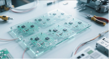
You might not realize it, but transparent glass PCBs are already in devices you use. Here are the most common applications:
Smartphone and Tablet Screens
The biggest use for transparent glass PCBs is in smartphone displays. Most modern OLED and AMOLED screens use a thin glass PCB with ITO traces to power the pixels. This is why your phone screen is clear— the PCB under it is transparent, so you only see the pixels, not the circuits.
For example: Samsung’s Galaxy S and iPhone 15 series use transparent glass PCBs in their displays. This lets them have thinner bezels and brighter screens, since the PCB doesn’t block light.
Smartwatches and Wearables
Wearables need small, lightweight, and attractive electronics—perfect for transparent glass PCBs. Smartwatches like the Apple Watch Ultra or Samsung Galaxy Watch use glass PCBs to power their displays and sensors. Since the PCB is clear, it doesn’t block the watch face, making the design look more seamless.
Some fitness trackers even use flexible glass PCBs—they bend with your wrist, making the tracker more comfortable to wear.
Smart Mirrors and Digital Signage
Smart mirrors (like the ones in bathrooms that show the weather or your calendar) use transparent glass PCBs to power the display behind the mirror. Since the PCB is clear, the mirror looks like a regular mirror when it’s off—and when it’s on, the display shines through without any visible circuits.
Digital signs (like the ones in malls or airports) also use glass PCBs. They let the signs be thinner and brighter, since the PCB doesn’t add bulk or block light.
Medical Devices
Medical monitors (like the ones in hospitals that show heart rate or blood pressure) need clear, reliable displays. Transparent glass PCBs are ideal here because they handle heat well (so the monitor stays cool during long use) and are easy to clean (glass is non-porous, unlike FR-4).
Some medical devices, like glucose monitors, also use small glass PCBs—they’re tiny enough to fit in portable devices, and the clear design makes them easier to sterilize.
Car Infotainment Systems
New cars are getting bigger, more advanced displays—from touchscreens on the dashboard to heads-up displays (HUDs) that project information onto the windshield. Transparent glass PCBs power these displays because they’re heat-resistant (important for hot cars) and can be shaped into curved designs (to fit the car’s interior).
For example: Tesla’s Model 3 and Model Y use glass PCBs in their central touchscreens. This lets the screen be thinner and more responsive, since the PCB doesn’t add extra thickness.
Are Transparent Glass PCBs Perfect? The Pros and Cons
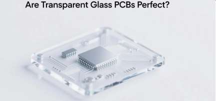
Like any technology, transparent glass PCBs have advantages and drawbacks. Let’s be honest about both so you can understand when they’re the right choice:
Pros of Transparent Glass PCBs
·Invisible design: Perfect for devices where you don’t want to see the circuit board.
·Heat-resistant: Handles high temperatures better than FR-4, making it ideal for bright screens.
·Flexible (thin versions): Bends slightly, great for wearables and foldable devices.
·Smooth and easy to clean: Glass is non-porous, so it’s good for medical or food-grade devices.
·Better light transmission: Doesn’t block light, so displays are brighter and more vibrant.
Cons of Transparent Glass PCBs
·More expensive: The manufacturing process (sputtering, photolithography) is complex, so glass PCBs cost 2-5x more than FR-4 PCBs.
·Fragile (if not thin): Thick glass PCBs can crack if dropped—though thin glass is more flexible, it’s still more fragile than FR-4.
·Less conductive than copper: ITO is a good conductor, but not as good as copper. This means glass PCBs aren’t great for high-power devices (like gaming PCs).
·Harder to repair: If the ITO layer gets scratched or damaged, it’s harder to fix than copper traces.
·Limited availability: Not all PCB manufacturers make glass PCBs—you might have to work with specialized factories.
The Future of Transparent Glass PCBs: What’s Next?
Transparent glass PCBs are still a relatively new technology, but engineers are already working on making them better. Here’s what to expect in the next 5-10 years:
Even Thinner, More Flexible Glass
Companies like Corning are developing glass that’s just 0.05mm thick—thin enough to fold like paper. This will let manufacturers make foldable devices (like phones or tablets) that bend more easily and last longer, since the glass PCB won’t crack.
Cheaper Manufacturing
Right now, sputtering (the process to add ITO) is expensive. Engineers are testing new methods, like printing ITO with inkjet printers, which would cut costs by 30-50%. If this works, glass PCBs could become as cheap as FR-4 PCBs—making them available for more devices.
Better Conductive Materials
ITO has a problem: it uses indium, a rare metal that’s getting more expensive. Scientists are testing alternatives, like:
·Silver nanowires: Almost as transparent as ITO, but cheaper and more conductive.
·Graphene: A super-thin, super-strong material that’s both transparent and an excellent conductor.
These materials would make glass PCBs more affordable and better at carrying electricity—opening up new uses (like high-power devices).
"Smart" Glass PCBs
Imagine a glass PCB that can change color, or sense touch, or even generate electricity from light. Engineers are integrating sensors and solar cells into glass PCBs, turning them into "smart" components. For example:
·A smart window that uses a glass PCB to adjust tint (blocking sunlight) and generate solar power.
·A touchscreen that uses the glass PCB itself to detect touches, no extra sensors needed.
More Sustainable Glass PCBs
Right now, making glass PCBs uses a lot of energy. Factories are working on greener methods, like using recycled glass for the substrate or using less energy in the sputtering process. This will make glass PCBs better for the environment—important as more devices use them.
Final Thoughts: Why Transparent Glass PCBs Matter
Transparent glass PCBs aren’t just a "cool" technology—they’re changing how we think about electronics. For decades, PCBs were hidden away, seen as a necessary evil. But glass PCBs turn them into a design feature—something that makes devices more beautiful, more functional, and more seamless.
Think about it: In 10 years, we might not have "bezels" on any screens. Our smart home devices could look like pieces of art, not gadgets. Our wearables could be so thin and flexible, we forget we’re wearing them. All of this will be possible because of transparent glass PCBs.
If you’re a designer, a hobbyist, or just someone who loves gadgets, keep an eye on transparent glass PCBs. They’re not just for high-end phones anymore—they’re going to be everywhere.
The next time you look at your smartphone screen, take a second to appreciate the transparent glass PCB working behind it. It’s the invisible hero making your screen bright, thin, and beautiful.
Have questions about transparent glass PCBs? Drop a comment below—I’d love to hear from you!
FAQs
Q. Why is the cost of glass-based PCBs higher than that of traditional PCBs?
A. Glass-based PCBs typically use special glass materials, such as borosilicate glass, which are inherently more expensive than traditional FR-4 materials. Additionally, their manufacturing process requires specialized equipment and techniques, such as thin-film deposition and photolithography. The complexity and cost of these processes are relatively high, resulting in an overall higher cost for glass-based PCBs compared to traditional PCBs.
Q. Can glass-based PCBs be used in high-power applications?
A. Glass-based PCBs have relatively poor thermal conductivity. Although their heat dissipation can be improved through certain thermal design measures, they are generally not well-suited for high-power applications. If the substantial heat generated in high-power applications cannot be dissipated promptly, it may affect the performance and lifespan of the PCB, potentially leading to failures. However, with effective thermal management strategies, such as adding heat sinks or using thermally enhanced packaging, glass-based PCBs can still be used in applications where power levels are not extremely high.
Q. Can glass-based PCBs be bent?
A. Yes. By using thin and flexible glass substrates, flexible glass-based PCBs can be manufactured. Flexible glass-based PCBs not only retain the advantages of glass, such as high transparency and chemical resistance, but also meet the requirements of applications that involve bending, such as wearable devices or flexible displays.
Q. Can the manufacturing of glass-based PCBs use the same equipment as traditional PCBs?
A. No. Glass-based PCBs require specialized manufacturing equipment and processes, such as thin-film deposition and photolithography. Traditional PCB manufacturing equipment, including through-hole drilling or surface-mount technology (SMT) assembly machines, may not be compatible with the manufacturing of glass-based PCBs.
Q. How is soldering performed on glass-based PCBs?
A. Soldering on glass-based PCBs differs from that on traditional PCBs. Since transparent solder pads cannot be directly identified using automated optical inspection (AOI), special techniques must be introduced. These include infrared thermal imaging positioning, which achieves an accuracy of ±0.1 mm, or the pre-placement of conductive adhesive to reduce the visibility of solder joints while ensuring soldering quality and reliability.
Author: Jack Wang

