


PCB Peelable Solder Mask The Art of Temporary Protection in Electronic Assembly
Introduction
In the intricate world of PCB manufacturing, a temporary protective material that can be easily removed is quietly revolutionizing electronic assembly processes. Peelable solder mask is basically liquid masking tape, also known as a peelable mask, providing a simple and effective way to safeguard specific areas during manufacturing.
In printed circuit board manufacturing, the solder mask is a critical component that protects circuits and prevents short circuits. Among these, a special type of solder mask material – the peelable solder mask – plays an indispensable role in complex assembly processes and is also used in the surface finish process thanks to its unique temporary protection properties.
Whether during wave soldering, electroless plating, or other high-temperature or chemical processing steps, the peelable solder mask provides precise protection for sensitive components and cleans up completely after its task is done, leaving no trace.
What is Peelable Solder Mask?
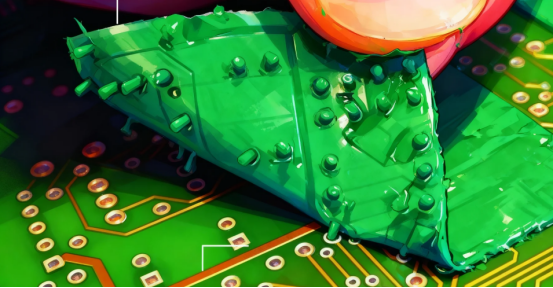
Peelable solder mask is a temporary protective material used to cover and protect sensitive or desired areas on printed circuit boards during specific manufacturing stages. Unlike traditional permanent solder masks, it can be easily manually removed after completing its protective mission without causing any damage to the PCB.
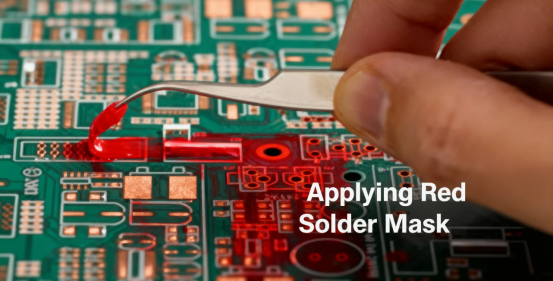
The PEEL OUT series produced by the German company Peters is a typical representative of peelable solder masks. Its application method can include screen printing or stencil printed techniques for precise coverage, allowing it to be economically applied to desired areas. This ensures that assembled PCBs are protected from direct contact with solder during wave soldering or electroless plating processes.
Core Characteristics of Peelable Solder Mask
1. Peelability
The most notable feature of peelable solder mask is its perfect peelability. After the soldering process, operators can easily remove it from the PCB surface without leaving sticky residues or damaging the board.
This characteristic makes it irreplaceable in complex PCB production requiring multiple soldering steps or staged assembly.
2. Exceptional Heat Resistance
Electronic soldering involves high-temperature environments, and peelable solder masks must withstand extreme temperatures. High-quality peelable solder masks like Peters' SD 2950 series offer high thermal stability, high elasticity, and tear resistance, capable of enduring the high-temperature processes of lead-free soldering and reflow soldering.
3. Precise Local Coverage Capability
Peelable solder masks support high-precision local application. Through screen printing technology, they can accurately cover specific areas needing protection, even hard-to-reach gold-plated rotary contacts can be covered and protected without issues.
This precision is particularly important for high-density interconnect boards.
4. Environmental Friendliness and Safety
Most modern peelable solder mask products use eco-friendly materials – solvent-free, VOC-free, silicone oil-free, grease-free, and acid-free – complying with RoHS standards and posing no harm to the environment or operator health.
Types of Masks
In the world of PCB assembly, selecting the right type of mask is crucial for ensuring the quality and reliability of the finished printed circuit board. There are several masking solutions available, each designed to meet specific needs during the pcb assembly process. The most common types include peelable solder masks, temporary solder masks, and high-temperature tapes.
Peelable solder masks are a popular choice for protecting selected areas of a printed circuit during wave soldering, reflow soldering, and surface finish processes. These masks are designed to be easily removed after the soldering process, leaving no residue behind and ensuring a clean, professional finish. Peelable solder masks are especially valued for their ability to withstand molten solder temperatures and extreme heat, making them ideal for use in high-temperature soldering processes, including those involving lead free solder.
Application methods for peelable solder masks are versatile. They can be applied using a squeeze dispensing bottle for manual control, a pneumatic system for higher volume production, or through screen printing and stencil printing for precise, repeatable coverage. The mask bottle can be held at an angle to apply a thick blanket of mask over larger areas, or upright to create a thinner strip for more targeted protection. However, applying the mask bottle upright at a 90° angle can sometimes force the mask through thru holes, increasing the risk of breakage or leaving residue, so care must be taken to avoid these issues.
Temporary solder masks are another option, designed to provide short-term protection during the typical wave soldering process. These masks are formulated to withstand melting point temperatures for about a second—just long enough to shield sensitive areas from molten solder during the soldering process. While they offer effective protection, they are generally not intended for prolonged exposure to high soldering temperatures or for use in reflow ovens.
High-temperature tapes are often used to protect larger or more delicate areas, such as gold fingers or connectors, from oxidation and excess solder during soldering processes. These tapes are manually installed and can be removed after the soldering process, but they may leave adhesive residue if not handled properly.
When choosing a mask for your pcb assembly, it’s important to consider the specific requirements of your process. For example, if your printed circuit board will be exposed to high soldering temperatures or molten solder temperatures, you’ll need a mask that can reliably withstand melting point temperatures up to 650°F (343°C) or higher. For complex designs with many thru holes, a peelable solder mask that can be easily applied and removed without leaving residue is often preferred.
Some of the most commercially available masks include products like WonderMASK P, known for its non-ammoniated, low-odor formula ideal for wave soldering, and Chemask, a fast-curing, peelable solder mask that can handle high temperature solder environments. These products are designed to be compatible with aqueous cleaning systems and are available in various thicknesses to suit different application needs.
Ultimately, the choice of mask depends on the soldering process, temperature profile, and design complexity of your printed circuit board. By selecting the right type of mask and following best practices for application—such as using the correct dispensing tip, controlling the thickness, and allowing for proper curing—you can avoid breakage, prevent residue, and ensure a smooth, reliable pcb assembly process.
Application Scenarios for Peelable Solder Mask
Protection During Wave Soldering
In wave soldering processes, peelable solder mask can protect already installed surface mount components from direct contact with molten solder. This is particularly important for mixed-technology boards containing both through-hole components requiring wave soldering connections and sensitive SMT components needing protection.
Protection During Electroless Plating and Surface Treatment
During electroless gold plating, silver plating, or other surface treatment processes, peelable solder mask can selectively mask specific areas, ensuring only required parts are plated, thereby improving product quality and reducing production costs.
Protection During Multiple Reflow Soldering
For complex assembly boards requiring multiple reflow soldering steps, peelable solder mask can protect already soldered areas during initial reflow steps, continuing to provide protection through subsequent soldering operations until all soldering processes are complete.
Protection of Gold Fingers and Connectors
Gold fingers and precision connectors on circuit boards are extremely vulnerable during soldering processes. Peelable solder mask provides perfect protection against solder splashing or chemicals affecting their surface properties and conductive performance.
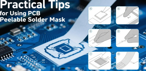
How to Use Peelable Solder Mask
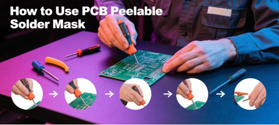
Proper use of peelable solder mask is crucial to ensuring its protective effectiveness:
1.Surface Cleaning: Thoroughly clean the PCB surface to remove contaminants like oil and dust, ensuring good adhesion of the peelable solder mask.
2.Precise Application: Apply the peelable solder mask evenly to areas requiring protection through screen printing, ensuring uniform thickness and complete coverage of target areas. A generally applied thinner layer can help avoid mask pushed into holes or around components, reducing the risk of breakage and residue.
3.Curing Process: Perform appropriate thermal curing according to product instructions to achieve sufficient adhesion and mechanical stability. A partially cured mask is more prone to increased brittleness or leaving residues, so complete curing is essential for optimal performance and removability.
4.Soldering Process: During wave soldering, electroless plating, or other processing, the peelable solder mask forms a physical barrier protecting underlying components and circuits. The mask must withstand high temperatures for a very brief time, often just around a second, during these processes.
5.Peeling Removal: After processing is complete and the board has cooled, manually peel off the solder mask, typically removing it completely in one piece without forced tearing. In high-volume settings, rotating brushes and other creative methods or devices may be used to facilitate efficient mask removal.
Comparison Between Peelable Solder Mask and Traditional Protection Methods
Compared to manually applied high-temperature tape, peelable solder mask offers significant technical and economic advantages:
·Significantly reduced application time, improving production efficiency
·No difficult-to-remove adhesive residues
·Automation capability through screen printing for more uniform coverage
·Ability to protect complex shapes and hard-to-reach areas
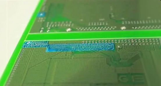
Common examples of peelable solder masks include the blue mask, which is a removable, in-process protective coating applied during PCB manufacturing to protect pads and holes during assembly.
Factors to Consider When Selecting Peelable Solder Mask
When choosing the appropriate peelable solder mask, consider the following factors:
·Thermal Stability: Must be suitable for specific soldering process temperatures, particularly high-temperature requirements of lead-free soldering. The ability to withstand extreme temperatures depends on the mask's formulation and application, especially during processes like wave soldering and reflow ovens.
·Correct Finish: Selecting the correct finish for exposed copper areas is essential to ensure proper solderability and protection, which is critical for the assembly process and overall PCB reliability.
·Chemical Resistance: Ability to withstand flux and other chemicals during soldering processes
·Elasticity and Tear Resistance: Ensures no cracking during thermal expansion and contraction, and easy complete removal
·Color and Contrast: Select colors that provide clear contrast with the substrate for easy inspection and rework
Technological Frontiers in Peelable Solder Mask Development
PCB protection technology continues to evolve, with peelable solder mask facing new innovation opportunities. For instance, in flexible electronics, researchers are developing polyimide-based peelable protective materials suitable for flexible PCBs.
Meanwhile, with advances in semiconductor technology, new surface treatment materials like gelatin-based polymer molecular brushes continue to emerge. These technologies promise to further simplify PCB manufacturing processes and improve protection performance in the future.
Practical Tips for Using Peelable Solder Mask
To fully leverage the performance of peelable solder mask, the following practical tips are worth noting:
·Preliminary Testing: Test compatibility between the peelable solder mask and specific PCB materials on small samples before large-scale application
·Thickness Control: Application that’s too thin may provide insufficient protection, while too thick affects heat transfer and increases removal difficulty
·Storage Conditions: Avoid storing peelable solder mask in high-temperature, humid environments to prevent affecting its performance. Always check the product's shelf life by referencing the batch code, manufacture date, and technical data sheet (TDS). The manufacture dates are often encoded in the batch code or provided in the technical data sheet, which also details essential product specifications.
·Complete Curing: Ensure curing process follows manufacturer recommendations to obtain optimal performance
·Reliability Testing: When using new or alternative peelable solder masks, conduct reliability testing to evaluate long-term performance and ensure suitability for your application.
Conclusion
As electronic devices continue developing toward miniaturization and higher density, the importance of peelable solder mask in PCB manufacturing and assembly will continue growing. Its precise protection characteristics make it an indispensable process material for manufacturing high-reliability electronic devices.
Whether for consumer electronics, automotive electronics, or precision circuits in aerospace applications, peelable solder mask will continue quietly guarding the safety of each precision component behind the scenes. After completing its protective mission, it departs quietly without leaving traces – gone but certainly not forgotten.
FAQs
Q. What is PCB peelable solder mask?
A. It is a temporary functional solder mask material. After application and curing, it protects specific areas of the PCB. Once the manufacturing step is complete, it can be completely peeled off without leaving residue or damaging the substrate.
Q. What is the core difference between it and traditional solder mask?
A. Traditional solder mask is permanent after curing, used for long-term protection. The peelable type is for "temporary protection"; it must be removed after the process is finished, serving only specific production stages.
Q. Where is it primarily used?
A. Local protection during wave soldering (preventing accidental soldering on pads); PCB rework and repair (protecting already soldered components); temporary shielding during multi-step assembly; preventing oxidation and scratches on gold fingers / test points; low-cost protection for small-batch PCBs.
Q. What are the common types?
A. Two main categories: Acrylic resin type (lower cost, easy peeling at room temperature, suitable for consumer electronics); Silicone resin type (high temperature resistance 260°C+, higher reliability, used in automotive/aerospace applications).
Q. What key specifications should be considered during selection?
A. High-temperature resistance (must match soldering temperatures); adhesion strength (5-15N/m, no residue after peeling); chemical resistance (resists flux/cleaning agents); film thickness (20-50μm, with a tolerance within ±5μm).
Q. Will peeling after application damage the PCB?
A. No, if the correct product is selected and applied properly. Peel slowly from a corner at a 30°-45° angle, avoiding excessive force. After peeling, gently wipe with isopropyl alcohol if needed.
Q. How much more expensive is it compared to traditional solder mask?
A. Approximately 3-5 times more expensive. However, it can reduce rework and cleaning costs, potentially lowering overall production expenses by around 20%.
Q. Can it be used on Flexible PCBs (FPCs)?
A. Yes, but a "flexible grade" must be selected (e.g., acrylic types containing elastomers). The film thickness should be controlled between 20-30μm to prevent cracking during bending.
Q. What are the storage requirements? Can it be reused?
A. Store in a cool, dry place (5-30°C, humidity ≤60%). Unopened shelf life is 6 months; use within 1 month after opening.
Reuse? No, it cannot be reused. After peeling, the film deforms and loses its adhesive properties. It is a single-use material.
Author: Jack Wang

