


Understanding PCB Buried Capacitance A Beginner-Friendly Guide to the Tech Changing PCBs
If you’ve ever opened a smartphone, laptop, or even a smart thermostat, you’ve held a printed circuit board (PCB) in your hands—those thin, green (or sometimes black) boards covered in tiny components that make electronics work. For years, PCBs relied on surface-mounted resistors and capacitors: small, chip-like parts glued or soldered to the board’s top or bottom. But as our devices get smaller, faster, and more powerful, those surface components are hitting a wall.
Enter buried resistance-capacitance (Buried RC)—a hidden hero of modern PCB design that’s solving some of the biggest headaches for engineers. Buried capacitance, in particular, is a technique used in PCB design and manufacturing to integrate capacitors within the layers of the board, improving high-frequency performance, reducing space, and enhancing power supply decoupling. In this guide, we’ll break down what Buried RC is, why it matters for your favorite gadgets, how it works (no PhD required!), and even who’s using it today. By the end, you’ll understand why this “invisible” tech is quietly revolutionizing everything from 5G phones to medical devices.
First Things First: What Are Resistors and Capacitors, Anyway?
Before we dive into “ buried” RC , let’s make sure we’re on the same page about the basics. Resistors and capacitors are two of the most common components in electronics—think of them as the “traffic cops” and “batteries” of a PCB:
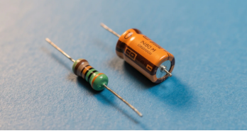
·Resistors: Slow down electrical current. Imagine a narrow pipe in a water system—resistors limit how much electricity flows through a circuit, preventing components (like your phone’s processor) from getting fried by too much power.
·Capacitors: Store and release electrical energy. They’re like tiny, fast-charging batteries that smooth out voltage spikes (ever noticed your laptop doesn’t crash when you plug in a charger? Thank capacitors!) and help signals travel reliably through the board.
In modern PCB design, engineers can use embedded capacitors within the internal layers of the board to achieve higher capacitance density, reduce parasitic inductance, and improve high-frequency filter performance, especially for power distribution networks.
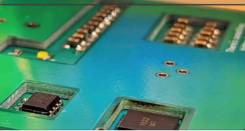
For decades, these parts were mounted on top of PCBs (called “surface-mount technology,” or SMT). But here’s the problem: As devices shrink (hello, ultra-thin laptops and tiny smartwatches), there’s less space on the PCB surface for these components. Engineers were stuck choosing between two bad options:
·Make the device bigger to fit more surface components, or
·Sacrifice performance by using fewer resistors/capacitors (which leads to glitchy signals or overheating).
·Buried RC solves this by putting resistors and capacitors inside the PCB—like hiding storage closets in the walls of a tiny apartment instead of piling boxes in the living room.
What Is Buried Resistance-Capacitance (Buried RC)?
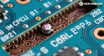
Buried RC is exactly what it sounds like: resistors and capacitors that are embedded (or “buried”) within the layers of a PCB, rather than mounted on its surface. Instead of sitting on top of the green board, these components are built into the PCB’s internal structure—specifically within the inner layer of the board, between the layers of copper and insulating material (called “dielectric”).
Think of a PCB as a stack of pancakes:
·Surface-mount components are like blueberries sprinkled on top of the stack.
·Buried RC components are like blueberries baked inside the pancakes—you can’t see them, but they’re still doing their job.
·This approach enables the integration of embedded passive components, such as resistors and capacitors, within the inner layers of the board to improve electrical performance and save space.
This simple shift (from “on top” to “inside”) fixes the space problem, but it also unlocks bigger benefits: faster signal speeds, less interference, and more durable devices. Let’s break down why that matters.
Why Buried RC Is a Game-Changer for Modern Electronics
You might be thinking: “So we’re just moving components inside—big deal?” But for engineers, Buried RC is a game-changer because it solves three critical challenges facing today’s electronics:
1. It Saves Precious Surface Space (No More Bulky Gadgets)
The average smartphone PCB is smaller than a credit card, yet it needs to power a screen, camera, 5G modem, and more. Surface-mount resistors and capacitors take up valuable real estate—each one is tiny (some are smaller than a grain of rice!), but hundreds of them add up.
Buried RC frees up the PCB surface for the components that need to be there: things like processors, sensors, and connectors. For example:
·A 5G phone’s PCB used to need 200+ surface resistors to manage signal flow. With Buried RC, 150 of those can be buried inside the board, reducing the need for discrete resistors—traditional, individually mounted resistor components—and freeing up even more board space for a larger battery or a smaller overall device.
·Medical devices like heart monitors (which need to be tiny and lightweight) use Buried RC to fit all critical components without sacrificing size—something surface-mount parts could never do.
·In short: Buried RC lets engineers make devices smaller or add more features (like better cameras or faster chips) without increasing the gadget’s size.
2. It Makes Signals Faster and More Reliable (Goodbye, Glitches!)
Ever had a video call freeze, or your laptop lag when you’re editing photos? Those issues often come from “signal loss” or “noise” on the PCB. Here’s why:
When electrical signals travel through a PCB, they can get disrupted by nearby components. Surface-mount resistors and capacitors are close to other parts (like copper wires), which creates interference—think of two people talking over each other in a crowded room.
Buried RC fixes this by:
·Placing resistors/capacitors right next to the components they power (e.g., a buried capacitor inside the PCB layer directly under the processor). This shortens the distance signals need to travel, making them faster.
·Reducing interference: Buried components are shielded by the PCB’s dielectric layers, so they’re less likely to “talk over” other signals. By embedding components within the PCB, buried RC also helps minimize cross talk, a form of electromagnetic interference that occurs between closely placed circuits and can degrade signal quality.
·For 5G and Wi-Fi 7 devices, this is a big deal. These technologies rely on ultra-fast signals (think: downloading a movie in 10 seconds), and even a tiny delay or glitch can ruin the experience. Buried RC ensures those signals stay strong and fast.
3. It Makes Devices More Durable (Less Likely to Break)
Surface-mount components are glued or soldered to the PCB’s surface, which means they’re vulnerable to damage. Drop your phone, and a surface resistor could pop off—leading to a dead camera or a glitchy screen.
Buried RC components are built into the PCB, so they’re protected from physical impact, moisture, and dust. This is a lifesaver for:
·Industrial equipment: Factory machines vibrate constantly—surface components would shake loose, but buried RC stays put.
·Automotive electronics: Cars endure extreme temperatures (from -40°F in winter to 120°F in summer) and bumps. Buried RC handles these conditions better than surface parts.
·Wearables: Smartwatches get wet, banged, and worn daily—buried components mean fewer repairs.
How Does Buried RC Actually Work? (Spoiler: It’s Not Magic)
The manufacturing process for embedding resistors and capacitors within printed circuit boards involves several advanced manufacturing processes, including precise layering, etching, and embedding steps. These processes allow manufacturers to embed resistors, capacitors, and even integrated circuit or integrated circuits directly into the PCB stack, enabling further miniaturization and improved performance.
You don’t need to be an electrical engineer to understand how Buried RC is made. Let’s walk through the process in simple terms—using our “PCB pancake stack” analogy again.
A standard PCB is made of layers: copper (for wires), dielectric (insulating material, like plastic), and a protective coating (the green stuff you see). The PCB stack includes both inner layers and outer layers, and embedded components are placed within these layers. To add Buried RC, manufacturers tweak this process in two key ways—one for resistors, one for capacitors.
To embed resistors, special equipment is required for precise placement and embedding within the PCB layers. Manufacturers can produce planar resistors using thin film technology such as OhmegaPly®, which is laminated into the board. These planar resistors are then subtractively processed from the thin film materials, typically using a resistor conductor material like a thin film NiP alloy. Selecting appropriate power ratings for embedded resistors is crucial to ensure reliable operation, especially in space-constrained environments. Embedded resistors provide more stability and can operate over a wide frequency range, making them ideal for high-frequency applications. Additionally, embedding resistors helps in reducing parasitic inductance, which improves signal integrity and overall circuit performance.
For capacitors, the manufacturing process involves embedding the capacitor plates within the PCB, and the capacitance can be measured per square inch of plate area. Other processes, such as lamination and quality control, are also critical to ensure the performance and reliability of the final printed circuit boards.
Step 1: Making Buried Resistors
Buried resistors aren’t separate “parts” like surface resistors. Instead, they’re made from special copper alloys (mixes of copper and other metals, like nickel or chromium) that naturally slow down electrical current (that’s the “resistor” job!).
Here’s how it’s done:
·Start with a layer of dielectric (the “pancake batter”).
·Etch (carve) a pattern into a sheet of copper alloy—this pattern will be the buried resistor.
·Glue this copper alloy layer to the dielectric.
·Add more layers of dielectric and copper (for wires) on top—hiding the resistor inside the stack.
·The beauty of this? The resistor can be shaped to fit exactly where it’s needed. For example, a tiny, curved resistor can be buried right next to a processor, no wasted space.
Step 2: Making Buried Capacitors
·Buried capacitors are a bit like tiny sandwiches inside the PCB. A capacitor needs two “plates” (to store charge) and an insulator between them—and that’s exactly how they’re built:
·Take two thin copper sheets (the “plates”).
·Put a layer of high-insulation dielectric (like ceramic or special plastic) between them—this is the “filling” that keeps the plates from touching.
·Glue this “sandwich” into the PCB stack, between other layers of copper and dielectric.
·Just like buried resistors, these capacitors can be sized to fit the device’s needs. A smartphone might use a tiny buried capacitor (1mm x 1mm) for its camera, while a car’s PCB could have a larger one for its battery management system.
Step 3: Testing to Make Sure It Works
Once the PCB is built, manufacturers test the buried components to ensure they work correctly. They use special tools to measure:
·Resistor value: Is the buried resistor slowing down current by the right amount?
·Capacitor capacity: Can the buried capacitor store enough energy?
·Connection: Are the buried components properly connected to the PCB’s wires?
If something’s off, they adjust the design—for example, changing the shape of the copper alloy for a resistor or using a thicker dielectric for a capacitor.
Designing with Buried RC: What PCB Designers Need to Know
When it comes to designing a printed circuit board with buried resistors and capacitors, engineers have a unique set of tools—and challenges—at their disposal. Unlike traditional designs that rely on discrete components mounted on the surface, embedding these passive components within the PCB layers opens up a world of possibilities for space saving and performance.
The first step in the design process is choosing the right materials. The dielectric material and its dielectric constant play a crucial role in determining how well the buried resistors and capacitors will perform. The thickness of each PCB layer must be carefully calculated to achieve the required resistance value and capacitance, ensuring that signals travel at high speed with minimal loss.
One of the biggest advantages of using buried resistors is their thin film nature. Because these components are formed as ultra-thin layers within the board, they help reduce parasitic inductance and electromagnetic interference—two major culprits behind signal crosstalk and degraded signal integrity. This is especially important in high-speed circuits, where even tiny disruptions can cause big problems.
PCB designers also need to think about the placement of these embedded components. Strategic positioning within the circuit board can help with impedance matching, further improving signal transmission and reducing the risk of glitches. By embedding resistors and capacitors exactly where they’re needed, designers can optimize the board’s performance while freeing up valuable surface space for active components.
In short, designing with buried RC isn’t just about saving space—it’s about creating a high-performance, reliable circuit that meets the demands of today’s electronics. With careful attention to materials, layer thickness, and component placement, PCB designers can unlock the full potential of buried resistance and capacitance in their next project.
Keeping Cool: How Buried RC Affects Heat Distribution
Thermal management is a critical factor in modern PCB design, especially as devices become more powerful and compact. By embedding resistors and capacitors within the PCB layers, buried RC technology offers a smart solution for distributing heat more evenly across the circuit board.
When resistors and capacitors are buried inside the board, heat generated by these components is spread throughout the surrounding layers, rather than being concentrated in one spot. This even heat distribution helps prevent hotspots that could damage other components or lead to premature failure. For high-performance applications—like medical devices, where stability and reliability are non-negotiable—this is a game changer.
The benefits don’t stop there. With improved heat distribution, designers can often eliminate the need for bulky heat sinks or additional cooling systems, saving even more space and simplifying the overall design process. This makes it easier to create compact, efficient PCBs that can handle demanding workloads without overheating.
By considering the thermal implications of buried resistance and capacitance during the design phase, engineers can ensure that their circuit boards not only perform better but also last longer. Whether you’re working on a cutting-edge medical device or a high-speed computing application, embedding resistors and capacitors is a smart way to keep your PCB—and your innovation—running cool under pressure.
Who’s Using Buried RC Today? (Spoiler: Your Favorite Brands)
Buried RC isn’t just a “future tech”—it’s already in the devices you use every day. Here are some of the biggest industries and products relying on it:
1. Consumer Electronics (Phones, Laptops, Wearables)
·Apple & Samsung: Their latest iPhones and Galaxy phones use Buried RC to fit 5G modems and larger batteries in tiny cases. Without Buried RC, those phones would be thicker or have shorter battery life.
·Laptop Makers (Dell, Lenovo): Thin-and-light laptops (like the Dell XPS or Lenovo ThinkPad) use Buried RC to free up space for faster processors—no more bulky “gaming laptop” designs for powerful machines.
·Wearables (Fitbit, Apple Watch): These tiny devices need to be durable and small. Buried RC lets them fit heart rate sensors, GPS, and batteries without breaking when you workout or swim.
2. Automotive (Electric Cars, Self-Driving Tech)
Electric vehicles (EVs) and self-driving cars have more PCBs than ever—think: battery management systems, radar, and touchscreens. Buried RC is critical here because:
·It handles extreme temperatures (EV batteries get hot, and winter cold can damage surface components).
·It saves space: EVs need every inch for batteries, so smaller PCBs mean more range.
·Companies like Tesla, Ford, and Toyota all use Buried RC in their latest EV models.
3. Medical Devices (Heart Monitors, Insulin Pumps)
Medical devices need to be tiny, reliable, and sterile. Buried RC is perfect for:
·Heart monitors: These devices are worn on the body and need to withstand movement—buried components don’t pop off.
·Insulin pumps: They deliver life-saving medication, so glitches from signal interference are dangerous. Buried RC ensures consistent performance.
·MRI machines: These use powerful magnets that can disrupt surface components—buried RC stays protected.
4. Industrial & Aerospace (Factory Machines, Satellites)
·Factory Equipment: Machines in factories vibrate and get dirty—surface components break easily, but buried RC lasts longer, reducing downtime.
·Satellites: Space is harsh (extreme cold, radiation, no air). Buried RC components are shielded from these conditions, so satellites keep working for years.
Is Buried RC Perfect? The Pros and Cons

No tech is perfect, and Buried RC has a few tradeoffs. Let’s break them down honestly:
Pros:
Buried resistors offer significant advantages in space-saving, improved thermal management, and increased circuit integration compared to traditional resistor technologies. This makes them ideal for high-density PCB designs where board real estate and heat dissipation are critical.
Pros of Buried RC
·Saves space: The biggest win—lets devices get smaller or add more features.
·Faster signals: Critical for 5G, Wi-Fi 7, and self-driving tech.
·More durable: Less likely to break from drops, moisture, or vibration.
·Less interference: Fewer glitches in your gadgets.
Cons of Buried RC
·Higher cost: Making Buried RC PCBs is more complex than surface-mount ones (you need special materials and tools). This means devices with Buried RC might be a little more expensive (though the cost is dropping as the tech becomes more common).
·Harder to repair: If a buried component fails, you can’t just solder a new one on—you might need to replace the entire PCB. That’s why it’s mostly used in devices where reliability is more important than repair cost (like medical devices or satellites).
·Not for every device: Simple electronics (like a basic remote control) don’t need Buried RC—surface-mount parts are cheaper and work just fine.
The Future of Buried RC: What’s Next?

As our devices get even smaller and more powerful (think: foldable phones, AI-powered wearables, and fully self-driving cars), Buried RC will only become more important. Here’s what engineers are working on next:
·Even smaller buried components: Future PCBs could have buried resistors and capacitors smaller than a human hair—letting devices get tiny (like smart contact lenses!).
·Buried RC + 3D PCBs: Right now, PCBs are flat stacks, but 3D PCBs (shaped like cubes or curves) are coming. Buried RC will be key to fitting components in these weird shapes.
·Lower costs: As more manufacturers adopt Buried RC, the price of making these PCBs will drop—soon, even budget phones and gadgets will use it.
Final Thoughts: Why Buried RC Matters for You
You might never see a buried resistor or capacitor, but they’re making your gadgets better every day. Without Buried RC:
·Your phone would be thicker, have shorter battery life, or struggle with 5G.
·Your laptop would be bulkier (no more thin-and-light models with fast processors).
·Medical devices like insulin pumps would be less reliable.
Buried RC is a perfect example of “invisible innovation”—the tech you don’t notice, but can’t live without. The next time you pick up your phone or laptop, take a second to appreciate the tiny, buried components working behind the scenes to make it all happen.
If you’re an engineer, hobbyist, or just curious about how electronics work, keep an eye on Buried RC—it’s only going to get more exciting from here. And if you have questions (or want to share how you’re using Buried RC!), drop a comment below—I’d love to hear from you.
FAQs
Q. What is PCB embedded capacitance?
A. Simply put, it’s a technology that "hides" capacitors inside the inner layers of a PCB (sandwiched between copper and insulating layers), rather than mounting them on the surface. It’s like "burying" components into the circuit board—they’re invisible to the eye but function normally.
Q. What’s the difference between embedded capacitors and ordinary surface-mounted capacitors?
A. The biggest difference is the installation location: regular capacitors are mounted on the PCB surface, taking up space and being prone to damage; embedded capacitors are built into the inner layers, saving space, resisting interference, and providing drop and moisture resistance. However, they can’t be replaced individually during repairs.
Q. Do embedded capacitors affect PCB heat dissipation?
A. They actually help with it. Since they’re embedded in the inner layers of the PCB, the heat generated during operation disperses into the surrounding layers, preventing concentrated "hot spots" and reducing the risk of component damage due to overheating.
Q. Can embedded capacitors be repaired if they fail?
A. It’s very difficult to repair them individually. Because they’re hidden inside the PCB, they can’t be directly desoldered and replaced like surface capacitors. If damaged, the entire PCB board usually needs to be replaced. This makes them more suitable for high-reliability devices that require minimal maintenance.
Q. Are PCBs with embedded capacitors more expensive?
A. They are slightly more expensive. Manufacturing requires specialized materials (e.g., specific insulating layers) and precise processes (e.g., inner-layer etching and lamination). However, as the technology becomes more widespread, costs are gradually decreasing. Nowadays, many mid-to-high-end devices commonly use them.
Author: Jack Wang

