


Breakthrough in Miniaturized PCBA Manufacturing Defense Strategy Against Solder Bridging in PCB Assembly Processes
I. The Critical 0.1mm Battlefield
In the era of 5G smart hardware, PCB assembly density is increasing at an annual rate of 18%. As 0201 components become standard in PCBA manufacturing, solder bridging defects have evolved into a critical technical bottleneck. Key findings reveal:
1. PCB assembly layouts with over 5 solder joints per cm² face a 3.2x higher bridging risk.
2. PCBA products using 0.4mm-pitch BGA packages incur 70% higher rework costs.
3. 35% of early failures in miniaturized PCBA modules for wearables stem from hidden solder bridging.

(Diagram: Evolution of solder joint density in mainstream electronic products)
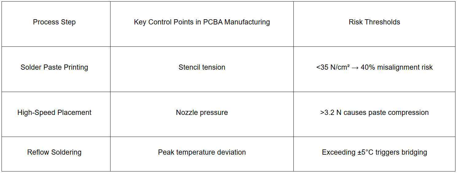
II. Full-Process Risk Analysis in PCB Assembly
1. Triple Traps in Design
① Component Layout Imbalance: A TWS earphone PCBA case study showed 85% of components concentrated on one side, causing reflow soldering offset.
② Pad Spacing Crisis: Bridging rates surge by 400% when 0402 component spacing falls below 0.25mm.
③ Solder Mask Defects: Failure to adopt micro-pitch SMD pads increases PCBA defect rates by 52%.
2. Invisible Killers in Manufacturing
3. Deadly Material Combinations
① Uncontrolled Paste Fluidity: PCB assembly-specific solder paste with viscosity <70 Pa·s reduces bridging by 65%.
② Stencil Deformation: Nano-coated stencils improve PCBA paste deposition accuracy to ±8μm.
③ Flux Residue: Low-residue formulations suppress hidden bridging risks below 0.3%.
III. Golden Protection System for PCBA Manufacturing
1. Intelligent DFM Design Matrix
① Establish PCB assembly component thermodynamics models (0.01mm² precision).
② Define spacing standards: 0402 ≥0.3mm, 0201 ≥0.2mm.
③ Implement stepped solder mask design (core area bridge width ≥0.08mm).
2. Process Control Triad
① Paste Printing Monitoring: 3D SPI systems detect thickness deviations (±10μm).
② Placement Pressure Control: Piezoelectric sensors enable 0.01N precision.
③ Dynamic Reflow Profiles: AI temperature control compensates for board warpage.
3. Material Innovations
① Nano-scale solder powder (D50=15μm).
② Self-aligning solder paste (28% optimized surface tension).
③ Low-temperature eutectic alloys (34°C lower melting point).
IV. Advanced Roadmap for PCB Assembly
1. Current Optimal Solutions
① Laser-assisted solder paste printing (<0.01% bridging rate).
② Hybrid selective wave soldering & hot air leveling.
③ X-Ray + AOI dual-mode inspection (detects 15μm defects).
2. Future Technology Roadmap
① Molecular-level solder resist coatings (contact angle >110°).
② Magnetically controlled self-assembly placement.
③ Digital twin-based PCBA virtual manufacturing systems.
V. Value Multipliers in PCBA Manufacturing
Implementing full-process control delivers:
1.First-pass yield >99.95%
2.PCBA rework costs reduced by 92%
3.Product lifecycle extended 3-5x
In the irreversible wave of miniaturization, companies mastering precision PCB assembly control are redefining PCBA manufacturing value chains. Partnering with nano-scale process experts will be decisive in the era of microelectronics.
(Data sources: IPC-7095D standard, ASM PT200 process white paper, Indium Corporation 2024 Solder Technology Annual Report)

