IC Substrate The Core Cornerstone of Chip Packaging, A Comprehensive Analysis from Technology to Applications
Behind electronic products such as smartphones, AI servers, and new energy vehicles, there is an “invisible hero” — the IC substrate. It serves as a “bridge” connecting chips to external circuits. Circuit boards act as the supporting structures for electronic components in these devices, providing connection, support, and heat dissipation across various applications. Without the IC substrate, even the most advanced chips cannot function. This article will use plain language to help you understand the core technology, application scenarios, and industry trends of IC substrates, uncovering the veil of this key link in the semiconductor industry chain.
What is an IC Substrate? Understand Its Core Function in One Sentence
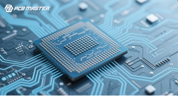
An IC substrate, fully known as Integrated Circuit Substrate, is a “high-precision substrate” specifically designed for chip packaging. Its core functions can be summarized in three points:
Physical Support: Fixes the chip to prevent damage during transportation and assembly;
Signal Interconnection & Electrical Connection: Enables high-speed signal transmission and provides reliable electrical connection between the chip and PCB (Printed Circuit Board) through internal fine circuits;
Heat Dissipation & Protection: Diverts heat generated by the chip and isolates external interferences such as moisture and dust.
To put it in a metaphor: If a chip is the “brain” of an electronic product, an IC substrate is the “brain’s exclusive carrier + signal hub” — it not only firmly holds the “brain” but also builds a communication channel between the “brain” and “other organs of the body” (such as screens and sensors), while also helping the “brain” cool down.
Unlike ordinary PCBs (printed circuit boards), IC substrates far surpass the former in precision and material performance: the line width/line spacing of ordinary PCBs is mostly 50-100 microns, while high-end IC substrates can be as small as 8 microns (equivalent to 1/10 the diameter of a human hair). Their wiring density is 10-20 times that of ordinary PCBs, which can meet the signal transmission needs of chips with thousands of pins.
IC substrates have different functions compared to other types of substrates or printed circuit boards, as they are specialized to provide high-density, reliable electrical connections and support advanced chip packaging technologies.
What Types of IC Substrates Are There? Choose the Right "Type" Based on Scenarios
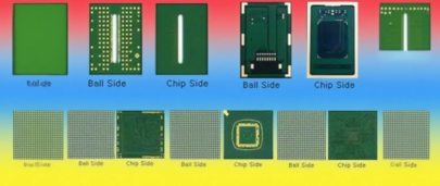
IC substrates can be classified mainly in two dimensions. One key classification factor is package type, which refers to the carrier form, packaging style, and bonding technology used. Package type significantly influences thermal performance, electrical characteristics, and application suitability across various IC package categories. Different types correspond to different packaging needs and application scenarios, and the selection should consider factors such as chip performance and equipment space.
Classified by Packaging Connection Method: Determines "How the Chip Connects"
WB Substrate (Wire Bonding Substrate)A traditional and low-cost connection method: uses 20-50 micron metal wires (gold wires, copper wires) to weld the chip’s pins to the substrate’s pads through heat and ultrasonic waves, forming a signal channel. Advantages: Mature manufacturing process, low cost; Disadvantages: Long signal path, relatively slow transmission speed. Suitable for scenarios with a small number of pins and low signal speed requirements. Applications: RF modules (mobile phone signal transceivers), memory chips (USB drives, memory cards), heart rate sensors in smartwatches.
FC Substrate (Flip Chip Substrate)The first choice for high-end chips: Flips the front side of the bare chip downward and directly connects it to the substrate through solder ball bumps (tens of microns in diameter) on the chip’s surface, realizing “point-to-point” high-speed transmission. As a type of chip package, FC substrate offers significant advantages such as low signal interference, high performance, and effective thermal dissipation compared to other packaging types. Advantages: Short signal path (80% shorter than WB), high transmission speed (50% faster), supports thousands of pins; Disadvantage: Relatively high cost. Applications: CPUs (computer processors), GPUs (graphics cards), high-end mobile phone SoCs (such as Snapdragon 8 Gen3, Apple A18).
BGA Substrate (Ball Grid Array Substrate)The bottom of the substrate is covered with solder balls, which connect to the external PCB through the solder balls. It has a large number of pins (hundreds to thousands), small pin spacing (minimum 0.4 mm), and strong stability. Applications: Server CPUs, industrial control chips (such as servo chips for CNC machine tools).
CSP Substrate (Chip Scale Package Substrate)The packaging size is close to that of the chip (no more than 1.2 times the chip area), achieving extreme miniaturization. Suitable for devices with limited space. Applications: Mobile phone camera sensors, wearable device chips (such as main control chips for smart bracelets).
Classified by Substrate Material: Determines "the Performance Ceiling of the Substrate"
Rigid Substrates (Accounting for Over 90%)
Rigid substrates are widely used in IC packaging, and the core material of these substrates is critical for determining their performance and suitability for different applications.
BT Substrate: A cost-effective option with good heat resistance (above 260℃) and insulation, and low cost. Suitable for mid-to-low-end scenarios, such as new energy vehicle engine control modules and ordinary mobile phone RF chips.
ABF Substrate: The “golden material” for high-end chips (developed by Ajinomoto of Japan). It has excellent insulation, low signal loss, and high wiring precision (below 8 microns). Ajinomoto Build-up Film (ABF) is a high-quality resin substrate material used in advanced IC packaging, supporting fine patterns and advanced manufacturing techniques such as the semi-additive process (SAP). It is the core choice for CPUs and GPUs, accounting for more than 70% of the global high-end IC substrate market.
Ceramic Substrate: Features high thermal conductivity (10 times that of BT substrates) and strong anti-interference ability. Ceramic substrates are made from ceramic materials such as aluminum nitride, silicon carbide, or alumina, which provide excellent thermal and electrical properties. Suitable for extreme environments, such as IGBT modules in new energy vehicles (high temperature resistance) and MRI equipment (magnetic field resistance).
The supporting core within multilayer rigid substrates provides structural stability and supports the intricate network of drill holes and conductor pads.
Flexible Substrates
Made of polyimide, they are bendable and lightweight. Suitable for foldable devices (such as display driver chips for foldable mobile phones) and medical equipment (such as pacemakers).
Core Advantages of IC Substrates: Why Can’t Chips Do Without Them?
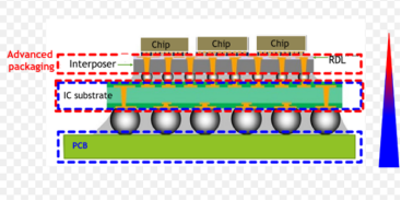
Ordinary PCBs can also connect chips, so why must high-end devices use IC substrates? Advanced IC substrates are essential for supporting high performance semiconductors, enabling complex packaging and high-density circuitry in modern electronic devices. The key lies in the fact that IC substrates solve four core pain points:
1. Space Utilization: "Maximizing Space in a Tiny Area"
Electronic products are becoming thinner, and internal space is extremely precious. The high-density wiring of IC substrates (8-micron line width/line spacing) can integrate thousands of pins in an area the size of a fingernail — if ordinary PCBs were used, the same function would require more than 10 times the area, which could not fit into devices such as mobile phones and watches at all.
2. Transmission Speed: A "High-Speed Road" for Signals
The improvement of chip performance relies on “fast signals”. By shortening the signal path (such as the solder ball connection of FC substrates) and optimizing materials (low signal loss of ABF substrates), IC substrates increase transmission speed by 50% and reduce loss by 30%, meeting the high-speed needs of 5G and AI chips. The precise formation of integrated circuitry on the substrate is crucial for achieving high-speed and reliable signal transmission, as it defines the electrical functionality and performance of the device. For example, BGA substrates used in 5G mobile phone baseband chips can avoid signal freezes; ABF substrates used in AI server CPUs can process tens of thousands of data streams simultaneously.
3. Low Resistance & Low Inductance: Reducing Signal Interference
Resistance and inductance can cause signals to "weaken" and "distort". IC substrates use high-purity electrolytic copper (with resistance only 1/2 that of ordinary copper) and multi-layer shielding design, reducing resistance by 40% and inductive interference by 50%, ensuring the precise operation of industrial control and medical equipment (e.g., CNC machine tools with an error controlled within 0.1 mm).
4. Heat Dissipation Capacity: A "Cooling Tool" for Chips
When chips operate at full load, their temperature can reach 80-100℃. Through designs such as high thermal conductivity materials (ceramic substrates) and embedded copper blocks, IC substrates increase heat dissipation efficiency by 80%. For example, ceramic substrates used in IGBT modules of new energy vehicles can control the temperature below 80℃, avoiding power failures.
How Are IC Substrates Manufactured? Focus on 3 Key Process Links
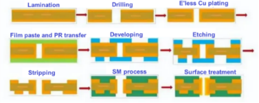
The manufacturing of IC substrates is a “micron-level precision project”, with core difficulties in “fine circuits” and “multi-layer stacking”. The fabrication process of IC substrates involves a series of precise steps required to create high-performance substrates for advanced electronic applications. As the IC package substrate plays a crucial role in chip packaging and manufacturing by providing a supportive and conductive layer for high-density integration, its production demands strict quality control. Additionally, the complexity and advanced technical requirements of IC substrate PCBs present greater manufacturing challenges and inspection needs compared to standard PCBs. We will focus on the three most critical links:
1. Circuit Fabrication: Two Mainstream Processes
Subtractive Process: First lay copper foil on a copper clad laminate, then etch away the excess part. Dry film is applied as a photoresist coating during etching and copper patterning to protect specific circuit areas. However, lateral etching can occur, causing the copper to etch sideways, which reduces circuit precision and limits minimum track widths. This process is suitable for mid-to-low-end substrates (WB, BT substrates) with relatively low precision (line width/line spacing ≥25 microns).
Additive Process (SAP): The mainstream for high-end substrates. First deposit a thin copper layer, then “draw” circuits through photolithography and the electroplating process, with precision reaching below 8 microns. Flash etching is used to define fine circuit patterns and remove seed layers with high precision. Additive printing is widely used in advanced electronics manufacturing to create high-precision components for SiP modules, BGA, and FCCSP. It accounts for 80% of ABF substrate production. For example, the substrate of NVIDIA A100 chips uses the SAP process, with a circuit precision of 10 microns.
2. Multi-Layer Stacking: A "Precision Puzzle" with 20+ Layers
High-end IC substrates require more than 20 layers of circuits, and the alignment error between layers must be ≤5 microns (1/10 the diameter of a human hair). During manufacturing, the process of "drilling - metallization - wiring" needs to be repeated, and each layer must be accurately matched; otherwise, short circuits will occur and the substrate will be scrapped. Currently, only enterprises from Japan and Taiwan, China can stably produce 20-layer ABF substrates.
3. Key Inspection: Controlling Millimeter-Level Errors
Finished products must pass three major inspections: appearance (no burrs or deviations), electrical performance (smooth signal transmission), and dimensions (tolerance ≤0.1 mm) to ensure precise assembly with chips and PCBs.
Essential Design and Production Techniques in IC Substrates
The design and production of ic substrates require a meticulous approach, combining advanced engineering with precise manufacturing processes. Leading ic substrate manufacturers begin by selecting the ideal substrate core and insulating materials, such as epoxy resin, BT resin, or high-performance ceramics, to match the specific requirements of the ic package. The choice of substrate material directly impacts electrical performance, thermal expansion, and overall reliability.
Layer stacking is another crucial aspect, as modern ic substrate production often involves building up multiple layers—sometimes more than 20—to accommodate complex copper circuitry and support high pin count ic chips. The arrangement and sequence of these layers are carefully engineered to minimize signal interference, optimize heat dissipation, and ensure robust electrical connections between different layers and components.
Bonding technology is tailored to the application: wire bonding is favored for cost-effective, lower pin count packages; flip chip bonding is chosen for high-speed, high-density applications; and tape automated bonding is used for specialized requirements. Each bonding method requires precise alignment and surface treatment to guarantee strong, reliable connections between the ic chip and the substrate. By mastering these essential design and production techniques, ic substrate manufacturers deliver substrates that meet the demanding standards of today’s electronics industry.
Copper Patterning and Plating: Crafting the Conductive Pathways
At the heart of every ic substrate is a network of copper circuitry that enables high-speed signal transmission and efficient power distribution. The ic substrate manufacturing process relies on advanced copper patterning and plating techniques to create these intricate pathways. Initially, a thin copper layer is applied to the substrate, and then precise copper patterning is achieved through methods such as photolithography, subtractive etching, or the semi-additive process (SAP).
Electroplating is commonly used to build up the copper layer, allowing for the formation of high-density, fine-line copper circuitry essential for high performance ic packages. The quality and uniformity of the copper layer are critical, as any defects can lead to signal loss, increased resistance, or even failure of the ic chip. By optimizing the copper patterning and plating steps, ic substrate manufacturers ensure that each substrate delivers the electrical performance, reliability, and high density required for advanced applications in data centers, consumer electronics, and industrial systems.
Advanced Bonding and Packaging Technologies
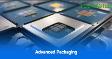
The evolution of ic packaging has been driven by the need for higher performance, greater miniaturization, and improved reliability. Advanced bonding and packaging technologies are at the forefront of this transformation, enabling the integration of multiple chips and multiple layers within a single ic package. Flip chip technology, for example, allows the ic chip to be mounted directly onto the substrate using solder bumps, resulting in shorter signal paths, lower power consumption, and reduced signal interference.
3D packaging takes integration a step further by stacking multiple layers of ic chips and substrates, saving space and boosting performance for applications like AI servers and wearable devices. Wafer-level packaging streamlines the manufacturing process by encapsulating the ic chip at the wafer stage, increasing yield and enabling the production of ultra-compact, high performance packages. These advanced technologies are essential for meeting the demands of modern electronic devices, from smartphones to automotive electronics, and are a key focus for ic substrate manufacturers seeking to push the boundaries of what’s possible in the semiconductor industry.
Flip Chip Technology: Direct Connections for Next-Gen Performance
Flip chip technology has revolutionized the way ic chips are connected to substrates, offering a leap forward in performance and miniaturization. By flipping the ic chip and attaching it directly to the substrate with an array of tiny solder bumps, this method eliminates the need for long wire bonds, dramatically reducing signal interference and enabling high-speed data transmission. The use of advanced substrate materials, such as silicon carbide and aluminum nitride, further enhances thermal conductivity and reliability, making flip chip packages ideal for high performance applications in data centers, AI servers, and cutting-edge consumer electronics.
Implementing flip chip technology requires precision in both the ic substrate manufacturing process and the bonding techniques used. IC substrate manufacturers must ensure perfect alignment, robust solder joints, and optimal surface treatment to achieve the desired electrical and thermal performance. As the demand for compact, high performance ic packages continues to rise, flip chip technology stands out as a cornerstone of next-generation electronic devices, enabling more powerful, efficient, and reliable integrated circuits.
Industry Status Quo & Future Trends: Booming Market, Technological Upgrading
Status Quo: Global Concentration, China Catching Up
Market Scale: The global IC substrate market reached 15 billion US dollars in 2023 and will exceed 20 billion US dollars by 2025. AI and new energy vehicles are the main driving forces (the unit price of AI chip substrates is 5-10 times that of ordinary substrates).
Competitive Pattern: Japan (Ajinomoto), Taiwan, China (Unimicron), and South Korea (Samsung Electro-Mechanics) monopolize more than 70% of the market. Mainland Chinese enterprises (Shennan Circuits, Fastprint Electronics) mainly focus on mid-to-low-end substrates, accounting for 15% of the market, and are currently breaking through ABF technology.
Bottlenecks: Mainland China relies on imported materials (ABF films) and equipment (laser drilling machines), and the yield rate of high-end substrates (80-85%) is lower than the international level (95%).
Three Future Trends
More Precise: Line width/line spacing will decrease from 8 microns to below 5 microns by 2027, requiring more advanced SAP processes and materials.
Greener: Lead-free surface treatment and recyclable materials will become popular, and energy consumption will be reduced (e.g., recycling etching solution).
More Integrated: "System-in-Package (SiP) substrates" will emerge, integrating CPUs, GPUs, and memory on a single substrate to reduce size (e.g., Apple’s A-series chips may adopt this in the future).
Conclusion: IC Substrates — The "Invisible Cornerstone" of the Semiconductor Industry Chain
From mobile phones to AI servers, and from new energy vehicles to medical equipment, IC substrates are the "last mile" for chip performance to be implemented. Without them, even the most advanced chip processes cannot be transformed into actual user experiences; without them, the miniaturization and high performance of electronic products would be empty talk.
With the boom in AI, 5G, and new energy vehicles, the demand for IC substrates will continue to grow. Technological upgrading (more precision, greener) and breakthroughs in localization will be the core themes of the industry in the future. Next time you use a fast-charging mobile phone or a smart car, you may remember — the IC substrate hidden behind the chip is silently supporting these convenient experiences.
FAQs
Q. What is the difference between an IC substrate and an ordinary PCB?
A. An IC substrate is a special type of PCB developed based on PCB technology. It has higher precision, smaller line width/line spacing, and better materials and functions, which can meet the needs of chips such as high-density signal transmission, while an ordinary PCB cannot meet these requirements.
Q. What are the respective characteristics of WB substrates and FC substrates?
A. WB substrates have a mature manufacturing process and low cost, but their signal transmission speed is relatively slow, and they are suitable for scenarios with a small number of pins and low signal speed requirements; FC substrates have short signal paths, high transmission speeds, and support a large number of pins. They are the first choice for high-end chips but have higher costs.
Q. What are the main substrate materials for IC substrates?
A. They mainly include rigid substrates (such as BT substrates, ABF substrates, and ceramic substrates) and flexible film substrates. Among them, rigid substrates account for more than 90%.
Q. What are the main difficulties in the manufacturing process of IC substrates?
A. They include forming the finest circuits on uneven surfaces, reducing defect rates, drilling micro vias at the correct positions, and maintaining the quality of ABF dielectric layers. All these place high requirements on manufacturing processes and equipment.
Why PCBMASTER: https://www.pcbmaster.com/why
Join US:https://www.pcbmaster.com/login

