


Mastering 0.25mm Pitch BGAs Precision Assembly Techniques for Success
Introduction
If you’re an electronics engineer, PCB designer, or managing smart hardware production projects, you’ve probably heard the term 0.25mm Pitch BGA – inspiring both love and hate.
Imagine a chip the size of a fingernail (like a smartphone processor or a drone sensor) with hundreds of pins densely packed on its underside. The distance between the centers of two adjacent pins is just 0.25mm – barely thicker than a human hair (approx. 0.05-0.1mm), maybe even fitting 2-3 hairs in that gap. Precisely mounting such a chip onto a PCB and ensuring every solder joint is robust and free of shorts is indeed a significant challenge for SMT (Surface Mount Technology). Only manufacturers with advanced assembly capabilities, including high-precision equipment and strict process control, can reliably handle such fine-pitch BGA components.
But now, 0.25mm Pitch BGA is no longer exclusive to “high-end equipment”: from budget smartwatches to industrial PLC modules and small sensors in medical devices, its advantages of “saving space, high integration, and low power consumption” have made it a “standard feature” in many products. Many engineers stumble during their first encounter – too much solder paste causing bridging, misalignment causing cold solder joints, leading to reworking entire batches, wasting time and increasing costs. Increased costs are often associated with pushing the limits of fine-pitch BGA assembly, as higher scrap rates and tighter tolerances make quality control more challenging.
Don’t worry. This article will thoroughly explain SMT assembly for 0.25mm Pitch BGAs from three perspectives: “what it is, why it’s difficult, and how to solve it.” Even if you’re new to the field, reading this will help you avoid 90% of the pitfalls and easily improve your assembly yield.
I. First, Understand: What exactly is a 0.25mm Pitch BGA? Why is it so common now?
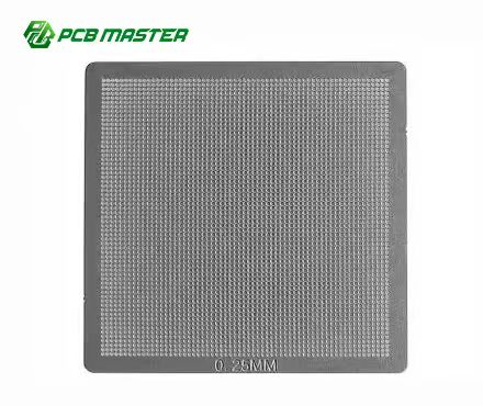
Before discussing assembly, we must clarify: What is “Pitch”? Simply put, “Pitch” is the center-to-center distance between the chip’s pins, measured in millimeters (mm). 0.25mm Pitch means the center distance between two adjacent BGA pins is only 0.25 millimeters.
Why has 0.25mm Pitch BGA become mainstream?
BGA (Ball Grid Array) packaging itself saves more space than traditional QFP (Quad Flat Package) – QFP pins are on the perimeter, while BGA pins (solder balls) are arranged in a grid array on the chip’s underside. A chip of the same size can fit more pins with BGA. BGA is a type of surface mount packaging, and unlike other surface-mount packages, BGA connects to the PCB through solder balls on the bottom, enabling higher density and more reliable connections.
The 0.25mm Pitch represents a golden balance between “integration” and “manufacturability”:
·More space-efficient than 0.3mm Pitch: For example, a 10mm×10mm BGA can fit about 600 solder balls at 0.3mm Pitch, but nearly 900 at 0.25mm Pitch, increasing integration by 50%. This is ideal for space-constrained devices like phones and earbuds.
·Easier to produce than 0.2mm Pitch: The 0.2mm Pitch spacing is too close (about the width of two human hairs), requiring higher precision in solder paste printing and component placement, making yield control harder and costs significantly higher. 0.25mm Pitch strikes a balance between “small size” and “ease of production,” making it the preferred choice for mid-to-high-end electronic devices.
·BGA technology enables higher connection density and reliability in modern PCB assembly, making it a preferred solution for advanced electronics.
The chips in your wireless earbuds, the MCU in your car’s infotainment system, and even the signal processing chip in your home router are likely 0.25mm Pitch BGAs – they’re already pervasive in our daily lives. Most manufacturers have mastered BGA technology for high-quality PCB assembly, ensuring that these components meet or exceed industry standard requirements.
SMT Challenges of 0.25mm Pitch BGA: More “Precise” Than You Think
Why do many engineers find 0.25mm Pitch BGA difficult to assemble? The core issue is one thing: “The space is too small, the tolerance for error is too low.”
A clear example: If during solder paste printing, each pad gets an extra 0.05mm of paste (about the thickness of a hair), it might not touch adjacent pins on a 0.3mm Pitch BGA. But on a 0.25mm Pitch BGA, with only 0.25mm between pins, the excess paste will directly connect two pins, causing “bridging” (a short circuit).
Another example is placement accuracy: If the XY-axis error of the SMT machine exceeds 0.03mm, and the chip shifts slightly, the solder balls might not align perfectly with the PCB pads, resulting in “cold solder joints” – intermittent connections after power-on, causing erratic device behavior that’s notoriously difficult to troubleshoot (because BGA solder joints are hidden underneath, invisible to the naked eye, requiring X-Ray inspection). Inspecting BGA components is complex due to their placement under the chip, making traditional optical methods insufficient for detecting soldering defects.
In summary, the SMT challenges of 0.25mm Pitch BGA focus on three stages:
·Solder Paste Printing: The amount of paste is critical – “a little too much or a little too little won’t work”.
·Component Placement: The chip must be precisely aligned with the pads, with error not exceeding 0.02mm.
·Solder Joint Inspection: Joints are invisible, requiring specialized equipment (X-Ray, AOI) for judgment, increasing the risk of missed defects. Automated X-ray inspection is essential for detecting hidden solder joint defects in BGA components, as it provides high detection accuracy where traditional optical methods fall short.
II. Practical Guide: 5 Steps to SMT Assembly for 0.25mm Pitch BGA (With Pitfall Avoidance Tips)

Actually, mastering the key steps makes SMT assembly for 0.25mm Pitch BGA manageable. With 10 years in SMT, having assembled hundreds of batches of 0.25mm Pitch BGAs, moving from an initial yield of 80% to a stable 99%+, I’ve developed a “standardized process” that even beginners can follow.
Step 1: Choose the Right Solder Paste – “Fine Particles” are Key
Solder paste is the “soul” of BGA assembly. Get it wrong, and subsequent steps are wasted. For 0.25mm Pitch BGA, paste must meet two core requirements: fine particles and good rheology.
·Particle Size: Prioritize lead-free solder paste (environmental regulations are strict, leaded paste is rare now) like Type 5 or Type 6. Type 5 particles are 20-38 microns in diameter, Type 6 are 10-25 microns, finer than Type 4 (38-50 microns). This allows precise filling of the 0.25mm Pitch gaps without easily causing bridging.
·Pitfall: Do NOT use Type 4 or coarser pastes! A client used Type 4 to save money, resulting in paste particles bridging pads, causing a 15% bridging rate, necessitating full rework and costing nearly ten thousand yuan.
·Alloy Composition: Commonly used is SAC305 (96.5% Tin, 3% Silver, 0.5% Copper), melting point approx. 217°C, offers moderate flow and high joint strength, suitable for most 0.25mm Pitch BGAs. For high-temperature environments (e.g., automotive electronics), consider SAC405 (95.5% Sn, 4% Ag, 0.5% Cu) with a slightly higher melting point and better high-temperature resistance.
·Paste Viscosity: Choose paste with a viscosity of 150-200 Pa・s (at 25°C). Too thin, and it may flow causing bridges; too thick, and it won’t print evenly, leading to insufficient paste volume.
Also, pay attention to storage and handling: Store refrigerated (0-10°C), thaw for at least 4 hours before use (do NOT use a microwave!), otherwise bubbles in the paste can cause “skipped pads” during printing.
Step 2: Stencil Design – “Aperture” Determines 80% of Yield
The stencil is the “mold” for solder paste printing. For 0.25mm Pitch BGA, stencil design revolves around “aperture size” and “shape.” A difference of 0.01mm can affect yield.
·Stencil Thickness: Prefer a 0.12mm thick stencil. Thinner leads to insufficient paste; thicker increases bridging risk. If the BGA pad diameter is 0.15mm (typical range for 0.25mm Pitch BGA is 0.12-0.16mm), a 0.12mm stencil provides the “just right” paste volume.
·Aperture Size: Follow the rule: Aperture Diameter = Pad Diameter × 0.9. E.g., for a 0.15mm pad, use a 0.135mm (0.15×0.9) aperture. Why reduce by 10%? Solder paste slumps after printing; reducing the aperture prevents excess paste.
·Pitfall: Don’t make apertures the same size as the pad! A client used 0.15mm apertures, resulting in excessive paste and 20% bridging. Reducing apertures to 0.135mm brought bridging below 1%.
**Aperture Shape:**Circular apertures are better than square for 0.25mm Pitch BGA. Square aperture corners can trap paste, while circular apertures distribute paste more evenly, reducing bridging risk. For very tight pitches (e.g., peripheral pads on a 0.25mm Pitch BGA), consider “oval” or “rounded rectangle” apertures (e.g., long axis 0.14mm, short axis 0.13mm) to further reduce bridging probability.
·Stencil Material: Choose 304 stainless steel for good flatness (error ≤0.005mm) and low tendency to warp. For high volumes (e.g., over 1000 boards per run), consider “electropolished stencils” for a smoother surface, better paste release, and higher printing precision.
·It is crucial to use carefully selected materials and components for reliable BGA assembly, as the right choices in stencil and paste directly impact yield and solder quality.
Step 3: Printing Parameters – “Slower and Steadier”
Solder paste printing is the “high-risk stage” for 0.25mm Pitch BGA. Incorrect parameters cause immediate issues. Here’s a verified “standard parameter set” for reference:
**Squeegee Pressure:**5-8 N (Newtons), adjust based on stencil size. E.g., 6 N for a 12×18 inch stencil; 5 N for a smaller 6×8 inch stencil. Too much pressure scrapes too much paste, causing insufficiency; too little leaves residue.
**Print Speed:**20-30 mm/s (millimeters per second). Slower speed allows paste to fully fill the apertures. Trying 40 mm/s resulted in incomplete fill and 8% insufficient solder; reducing to 25 mm/s dropped it to 0.5%.
**Separation Speed (Snap-off):**1-2 mm/s (slow separation). This is crucial! If the stencil separates too quickly, paste can be “pulled out,” causing “webbing” and bridging. Slow separation lets the paste stay cleanly on the pads.
Printing Environment: Control temperature at 22-25°C, humidity at 40%-60%. High humidity causes paste to absorb moisture, leading to voids (bubbles) during reflow; low humidity dries the paste, degrading its flow properties.
Always perform First Article Inspection after printing: Use a microscope (20x magnification or higher) to check several pads for paste consistency, missing paste, or excess paste before proceeding with batch printing.
Step 4: Component Placement – “Precision to the Micron”
Placement accuracy for 0.25mm Pitch BGA is extremely high. XY error must not exceed ±0.02mm (20 microns), about one-third the width of a human hair. Achieving this requires two things: machine calibration and vision alignment.
·Machine Calibration: Always calibrate the SMT machine’s “nozzle” and “vision system” before placement. Use the correctly sized nozzle (e.g., a 10x10mm nozzle for an 8x8mm BGA). Replace worn nozzles promptly to avoid picking instability and misplacement. Calibrate the vision system using “Fiducial marks” (PCB reference points) to ensure accurate PCB positioning.
·Placement Force:****50-80 grams (g), adjust based on component weight. E.g., 50g for a small 5x5mm BGA; 70g for a larger 10x10mm BGA. Too much force damages the chip or PCB; too little doesn’t seat the chip firmly, risking movement during reflow.
·Placement Temperature: Room temperature is fine; heating is unnecessary. The tackiness of the paste itself holds the chip. Heating might prematurely melt the paste, causing misalignment.
An automated SMT production line, equipped with high end machines such as automated solder dispensers, pick-and-place machines, and advanced vision systems, ensures high accuracy, high yield, and quality control during the placement of 0.25mm pitch BGA components. High precision is required in all steps of 0.25mm pitch BGA assembly to achieve reliable results.
After placement, use X-Ray to check the “placement offset.” If offset exceeds 0.02mm, adjust machine parameters (e.g., vision alignment compensation values) until within specification.
Step 5: Reflow Profile – “Gradual and Controlled”
Reflow soldering is the key step where solder melts to form joints. The reflow profile for 0.25mm Pitch BGA must be “gentle,” avoiding rapid temperature spikes/drops that can damage components or cause voids. Here’s a “standard reflow profile” for SAC305 paste:
·Preheat Zone: Ramp from room temperature to 150-170°C at a rate of 1-2°C/s, lasting 60-90 seconds. Purpose: Allows solvents in the flux to evaporate, preventing spattering or bubbling later.
·Soak/Preflow Zone (Thermal Soak): Maintain temperature between 170-180°C for 60-120 seconds. Purpose: Allows the flux to activate fully, removing oxides from pad and ball surfaces. Also equalizes temperature across the PCB and component, minimizing thermal stress and warpage.
·Reflow Zone (Liquidus above): Ramp from 180°C to a peak temperature of 240-250°C at 2-3°C/s. Hold time at peak temperature (Time Above Liquidus - TAL) should be 20-30 seconds. Critical: Peak temp must not exceed 255°C (risk of chip damage) or be below 235°C (risk of incomplete melting, weak joints).
·Cooling Zone: Cool from peak temperature to below 100°C at a rate of 2-4°C/s, taking 30-60 seconds. Cooling too fast makes joints brittle; too slow promotes excessive intermetallic growth and oxidation.
A reflow oven is used for controlled heating and cooling profiles, ensuring consistent soldering results. During reflow, surface tension plays a crucial role in maintaining proper alignment of solder balls as they melt and solidify, which is critical for reliable BGA assembly.
After reflow, use X-Ray to inspect joint quality: Good joints should be “full, round, without voids or bridges.” Voiding should be controlled below 15% (higher voiding affects electrical conductivity and thermal performance). If voiding is high, adjust the reflow profile (e.g., extend soak time to allow better flux activity and outgassing).
The assembly of 0.25mm pitch BGAs is an automatic process requiring precise control and advanced equipment, including fully automated SMT and BGA soldering lines, to ensure high quality and yield rate.
III. Common Issues & Solutions: Fix These Common Pitfalls

Even with a standard process, issues can arise. Here are 5 common problems with specific solutions for quick troubleshooting.
1.Issue: BGA Misalignment after placement; balls not aligned with pads.Causes:
① Incorrect vision alignment (fiducial misrecognition)
② Worn nozzle, unstable pickup;
③ Placement force too low, chip not held firmly. Solutions:
·Check Fiducials: Clean fiducials with alcohol if dirty; recalibrate vision system if fiducial position is off.
·Replace Nozzle: Test with a new nozzle.
·Increase Placement Force: e.g., from 50g to 60g, observe if offset decreases.
2.Issue: X-Ray shows solder bridging (adjacent balls connected).Causes:
① Too much solder paste (stencil aperture too large or print pressure too low)
② Paste rheology too prone to flow during reflow
③ Placement misalignment bringing balls too close. Solutions:
·Reduce Stencil Aperture Size: e.g., from 0.14mm to 0.13mm.
·Use Higher Viscosity Paste: If using 180 Pa・s paste, try 200 Pa・s (Note: Check context, sometimes lower viscosity might be suggested for other flow issues, but generally higher viscosity resists bridging).
·Adjust Placement Accuracy: Calibrate machine, control offset within ±0.01mm.
3.Issue: High Solder Joint Voiding (>15%).Causes:
① Moisture in solder paste (improper storage or insufficient thawing)
② Reflow preheat zone too short, flux not fully volatilized;
③ Oily or oxidized PCB pads. Solutions:
·Check Paste: Ensure adequate thaw time; replace paste if expired.
·Adjust Reflow Profile: Extend preheat/soak time, e.g., from 60s to 90s.
·Clean PCB Pads: Wipe pads with alcohol; if severely oxidized, gentle abrasion (carefully avoid removing pad finish).
4.Issue: Cold Solder Joints / Insufficient Solder (intermittent connection, X-Ray shows non-full joints).Causes:
① Insufficient solder paste (stencil aperture too small or print pressure too high)
② Reflow peak temperature too low, paste not fully melted
③ Oxidized pads or balls, flux not activating sufficiently. Solutions:
·Increase Stencil Aperture: e.g., from 0.13mm to 0.135mm.
·Increase Reflow Peak Temperature: e.g., from 240°C to 245°C.
·Use Paste with Higher Flux Activity: e.g., paste with 12% flux content vs. standard 10%.
5.Issue: Fluctuating Yield in Mass Production.Causes:
① Inconsistent solder paste (viscosity varies between batches)
② Warped stencil (lost flatness over time)
③ Machine parameter drift (e.g., squeegee pressure decreasing gradually). Solutions:
·Test Paste Batches: Sample test each new batch of paste by printing 10 PCBs, check consistency.
·Regularly Inspect Stencil: Check stencil flatness weekly with a gauge; replace if warpage exceeds 0.01mm.
·Schedule Machine Calibration: Calibrate squeegee pressure, placement accuracy, etc., daily before production starts.
Process optimization and troubleshooting require building high quality assemblies through strict process control and advanced inspection methods. Effective inspection and process control can help reduce production costs by minimizing defects and rework.
IV. Future Trends: Will 0.25mm Pitch BGA be Replaced?

After reading this, you might ask: With rapid tech advancement, will 0.25mm Pitch BGA soon be replaced by finer pitch packages?
My answer: Not in the short term; it will become even more prevalent. Two reasons:
·High Cost-Effectiveness: 0.25mm Pitch BGA meets the integration needs of over 90% of mid-to-high-end devices, with assembly costs 30%-50% lower than 0.2mm Pitch. For most companies, it’s the “optimal cost-performance solution.”
·Optimizing Technology: SMT equipment is getting smarter (e.g., AI vision reducing placement error to ±0.005mm), and new pastes (e.g., nano-particle) are emerging for finer pitches. Future assembly of 0.25mm Pitch BGA will become easier with higher yields.
Of course, in areas demanding extreme miniaturization (e.g., micro medical sensors, space equipment), 0.2mm or even 0.15mm Pitch BGAs will gradually increase, but their volumes are small and costs high, not threatening the mainstream status of 0.25mm Pitch BGA. Leadless BGA is also one of the package options handled in advanced assembly lines, expanding the range of BGA assembly capabilities.
Introduction to Ball Grid Array
The Ball Grid Array (BGA) is a breakthrough in surface mount technology (SMT) that has transformed the way electronic components are packaged and assembled onto circuit boards. Unlike traditional packages that use leads or pins around the perimeter, BGA packages utilize an array of tiny solder balls on the underside of the component. This innovative approach allows for much higher pin density, making it possible to connect complex integrated circuits to the circuit board in a compact footprint.
BGA assembly technology offers several key advantages: it enables higher electrical performance by shortening the connection paths, reduces thermal resistance for better heat dissipation, and supports the miniaturization of electronic devices. As a result, BGA assembly services are now widely used across industries, from consumer electronics to the LED industry, where high accuracy and high yield are essential for success. The ability to reliably assemble BGAs has become a hallmark of modern SMT assembly, allowing manufacturers to meet the demands of today’s densely packed, high-performance electronic products.
BGA Package Types
BGA packages come in several varieties, each tailored to specific application needs and performance requirements. Ceramic BGA (CBGA) packages use a multilayer ceramic base material, offering excellent reliability and superior heat dissipation—making them ideal for high-performance or mission-critical applications. Plastic BGA (PBGA) packages, in contrast, use a plastic substrate, providing a more cost-effective solution for high-volume production while still delivering solid electrical performance.
For applications where space is at a premium, Micro BGA (μBGA) packages feature an even smaller ball pitch, enabling extremely high pin density in compact designs. The choice between ceramic BGA, plastic BGA, and micro BGA depends on factors such as required electrical performance, heat dissipation needs, and the importance of cost reduction. Ultimately, the right BGA assembly capability ensures that the selected package type delivers both reliability and value, supporting the demands of modern electronic assembly.
BGA Packaging Considerations
Designing and manufacturing a high-quality BGA package involves careful attention to several critical factors. The selection of the base material—whether ceramic or plastic—directly impacts the package’s thermal and mechanical properties. The design of the solder pads and the precise placement of solder balls are equally important, as they determine the integrity of the electrical connections and the overall reliability of the assembly.
To achieve the necessary precision, many manufacturers rely on automated solder dispensing machines and automatic placement machines, which help ensure consistent solder ball placement and alignment. Strict factory inspection protocols, including thorough testing and quality checks, are essential to catch any defects early in the process. Additionally, the minimum pitch size and minimum diameter of the solder balls must be carefully specified to match the requirements of the application and the capabilities of the assembly process. By addressing these BGA packaging considerations, manufacturers can deliver assemblies that meet the highest standards of quality and reliability.
Precision Assembly Techniques for 0.25mm Pitch BGAs
Assembling BGAs with a 0.25mm pitch pushes the limits of current SMT assembly technology, demanding both advanced equipment and expert process control. Automated SMT production lines equipped with the latest placement machines and AOI inspection systems are essential for achieving the high accuracy required at such fine pitches. Every step, from solder paste application to component placement and reflow soldering, must be precisely controlled to ensure robust solder joints and prevent defects.
The design of the solder mask and solder pads plays a crucial role in guiding solder flow and preventing bridging or voids. Reflow soldering profiles must be carefully tuned to match the thermal characteristics of the BGA package and the circuit board, ensuring complete wetting and strong, reliable connections. Professional engineers with deep experience in BGA assembly technology are indispensable for troubleshooting, optimizing processes, and building high-quality BGA assemblies. By leveraging the expertise of many professional engineers and the latest equipment, manufacturers can consistently achieve the high yields and reliability demanded by today’s most advanced electronic products.
Conclusion:
For 0.25mm Pitch BGA SMT, “Details” Determine SuccessActually, SMT assembly for 0.25mm Pitch BGA isn’t about “profound technology” but hinges on “details” – choosing the right paste, designing the stencil well, controlling printing and placement parameters, and conducting proper inspections. Master these, and you can handle it easily.
Professional BGA assembly service is invaluable for high-quality, reliable PCB assembly, as it leverages advanced technology, equipment, and inspection processes to ensure optimal results. The importance of monitoring solder quality and inspecting soldering joints beneath the BGA package cannot be overstated, as these are critical for reliable connections. The use of a combination inspection method—including electrical testing, boundary scan, and automated X-ray inspection—significantly improves detection accuracy for solder joint defects. Boundary scan is a non-destructive technique for verifying BGA solder joints, and electrical testing is used to verify the quality and reliability of BGA solder joints. Through hole inspection methods are also used for certain types of PCB analysis, complementing other inspection techniques. Using multiple inspection methods can improve detection accuracy for soldering defects, especially since traditional optical methods are limited for BGA inspection.
BGA technology supports a variety of BGA components and package types, including PBGA, CBGA, Micro BGA, and leadless BGA, and may use wire bonding as an alternative interconnection technique in BGA manufacturing. Advanced PCB manufacturers utilize high end machines and automated SMT production lines to achieve high-precision placement and inspection, meeting or exceeding industry standard requirements for BGA assembly. Precise control in every step of 0.25mm pitch BGA assembly is essential for optimal yield and reliability.
I’ve seen many newcomers initially afraid of 0.25mm Pitch BGA but, after following these steps, saw their yields jump from 80% to 99%. So don’t be afraid. Try it a few times, gain experience, and you too can become a “BGA assembly expert.”
If you encounter specific problems during actual operation, feel free to leave a comment; I’ll reply to each one. Also, share your assembly experiences – let’s learn and progress together!
Finally, remember to bookmark this article for reference the next time you assemble 0.25mm Pitch BGAs!
FAQs
Q. What is a 0.25mm pitch BGA?
A. It refers to a Ball Grid Array (BGA) package with a center-to-center distance between adjacent solder balls of 0.25mm. The solder balls are arranged in a grid pattern on the bottom of the chip. Its core advantages are "space-saving and high integration," making it widely used in mid-to-high-end electronic devices.
Q. What are the core challenges in its SMT assembly?
A. The key challenge is the "low fault tolerance": too much or too little solder paste can easily cause bridging or cold joints. The placement accuracy must be ≤ ±0.02mm, and hidden solder joints require specialized equipment for inspection.
Q. What type of solder paste is suitable for it?
A. Type 5/6 lead-free solder paste is preferred (particle sizes of 20-38μm/10-25μm). SAC305 alloy is commonly used, with a viscosity of 150-200 Pa·s (at 25°C).
Q. What are the key requirements for stencil design?
A. A thickness of 0.12mm is recommended. The aperture diameter should be 0.9 times the pad diameter. Circular apertures are preferred to avoid solder accumulation and bridging, which can occur with square apertures.
Q. How to inspect the quality of its solder joints?
A. Automated X-ray Inspection (AXI) is required. Key inspection points include bridging, voids (which must be ≤15%), and cold joints. Direct visual inspection is not possible.
Author: Jack Wang

