


What is 99.6% Alumina Ceramic Substrate PCB
Introduction to Ceramic Substrates
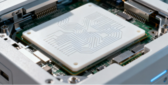
Ceramic substrates form the backbone of ceramic printed circuit boards, providing a robust and reliable platform for advanced electronic applications. Made from high-performance ceramic materials such as aluminum oxide (alumina) and aluminum nitride, these substrates are engineered to deliver exceptional thermal conductivity, making them ideal for environments where efficient heat dissipation is critical. The unique combination of physical and chemical properties found in ceramic substrates—such as high temperature resistance, outstanding wear resistance, and superior electrical insulation—ensures stable operation even under extreme conditions. Thanks to their ability to withstand high temperatures and resist thermal shock, ceramic substrates are widely used in a range of industrial applications, from power electronics to aerospace systems. Their excellent chemical properties and durability make them suitable for use in harsh environments, where reliability and longevity are paramount.
Product Specifications
·Material: Al₂O₃ 99.6% (High-purity alumina al ceramic substrate material)
·Thermal Conductivity: ≥30 W/(m·K)
·Dielectric Constant (1 MHz, 20 ℃): 9.9 ± 0.2
·Dielectric Loss (1 MHz, 20 ℃): ≤1×10⁻⁴
·Volume Resistivity (20 ℃): ≥1×10¹⁴ Ω·cm
·Flexural Strength: ≥500 MPa
·CTE (25–300 ℃): 7.0–7.5×10⁻⁶ / ℃
·Surface Roughness (Ra): ≤0.6 μm
·Flatness (Warp): ≤1‰ (polished)
·Max Working Temperature: 1500 ℃
Product Description
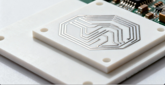
PCBMASTER presents the high-performance 996 Alumina Ceramic Substrate (Al₂O₃ 99.6%), engineered for high-power, high-frequency, and high-reliability electronic applications. With superior thermal conductivity, excellent insulation, and outstanding mechanical strength, it provides a stable and durable foundation for advanced semiconductor and power electronic devices.
The substrate delivers efficient heat dissipation (≥30 W/m·K) and a low dielectric constant (9.9±0.2), ensuring minimal signal loss and superior stability under extreme operating conditions due to its excellent electrical properties and low loss tangent, which are critical for high-frequency, RF, and microwave applications. Its tight dimensional tolerance and high flatness make it ideal for precision packaging and multilayer module assembly. The substrate can also be manufactured in a variety of shapes to accommodate specific design requirements.
Additionally, the alumina ceramic substrate offers more easy handling during manufacturing and assembly, improving process efficiency.
Key Features
The following are the key advantages of the alumina ceramic substrate:
·High thermal conductivity ≥30 W/(m·K): Enables efficient heat dissipation for power devices
·Low dielectric constant (9.9±0.2): Minimizes signal loss in high-frequency circuits
·High flexural strength ≥500 MPa: Ensures excellent mechanical reliability
·Ultra-high purity Al₂O₃ 99.6%: As one of the most effective insulating materials for electronic applications, it provides stable electrical insulation and long service life
·Low dielectric loss ≤1×10⁻⁴: Supports high-speed and low-loss signal transmission
·Excellent CTE match (7.0–7.5×10⁻⁶/ ℃): Compatible with semiconductor materials
·Superior flatness ≤1‰ (polished): Ensures precision in assembly and bonding; the substrate can be produced in a variety of shapes to meet different application needs
·Surface roughness ≤0.6 μm: Suitable for fine-line circuit printing
Design Considerations
When developing ceramic PCBs, careful attention must be paid to material selection and design parameters to achieve optimal results. The choice of ceramic substrate—whether alumina for its high thermal conductivity and relatively low cost, or silicon carbide for its superior mechanical strength—depends on the specific requirements of the application. Designers must also consider the manufacturing process, including how conductive traces are applied and which surface finishes are used, as these factors influence both performance and cost. Matching the coefficient of thermal expansion (CTE) of the ceramic substrate with that of the conductive materials is essential to prevent thermal stress and ensure long-term reliability, especially in applications exposed to frequent temperature fluctuations. By balancing these considerations, engineers can leverage the unique properties of ceramic materials to create ceramic PCBs that offer high mechanical strength, low dielectric loss, and excellent thermal management at a competitive cost.
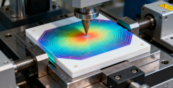
Surface Finish and Manufacturing
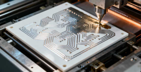
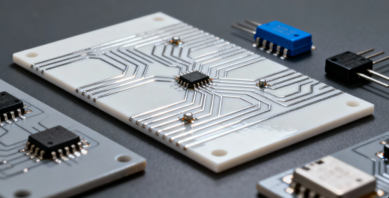
The surface finish of a ceramic PCB plays a vital role in its electrical performance and long-term reliability. A smooth, high-quality surface finish ensures optimal electrical contact and helps protect against corrosion, which is especially important in demanding industrial environments. Copper metallization is a widely used surface finish for ceramic substrates, offering excellent electrical conductivity and compatibility with various assembly processes. The manufacturing process for ceramic PCBs typically involves several key steps: producing the ceramic substrate, applying conductive traces using thick film or thin film techniques, and adding the desired surface finish. Each stage must be carefully controlled to achieve the required properties and performance. Collaborating with experienced production partners who understand the nuances of ceramic PCB manufacturing can help ensure adherence to design rules, material selection, and quality standards, resulting in ceramic PCBs that meet the highest expectations for reliability and functionality.
Applications
The alumina ceramic substrate is a core component in advanced ceramic pcb solutions for demanding industries, offering superior thermal, electrical, and mechanical properties.
·Power electronics (IGBT, MOSFET modules) – These modules often operate at elevated temperatures, making the substrate highly suitable for reliable performance.
·Automotive electronics and EV power modules
·RF and microwave communication systems – Widely used in high frequency applications due to their precise electrical properties and efficiency.
·Industrial control and inverter systems
·Aerospace and defense electronic packaging
For medium- to high-volume manufacturing, C production is available to ensure consistent quality and supply for large-scale projects.
Conclusion
In summary, the 99.6% alumina ceramic substrate provides a solid foundation for addressing the challenges of thermal management and signal integrity in modern electronic devices through its exceptional thermal conductivity, electrical insulation, mechanical strength, and long-term reliability. It stands as one of the preferred materials for engineers seeking higher performance, smaller dimensions, and extended lifespan in demanding applications, with its value being particularly irreplaceable in high-power and high-frequency scenarios.
FAQs
Q. What are the core composition and purity characteristics?
A. The primary composition is Al₂O₃ with a purity of 99.6%, while the remaining 0.4% consists of trace impurities. The high purity minimizes adverse effects on performance.
Q. What are the key performance features?
A. High thermal conductivity, excellent electrical insulation, high-temperature stability (withstands 1500–1700°C), high flexural strength, low dielectric loss, and low surface roughness (as low as ≤0.6 μm in some cases).
Q. Which processing techniques are suitable?
A. It can be laser-processed, thin-film metallized (e.g., sputtering/evaporation), and some variants allow cutting and drilling (requires compatible processes).
Q. What are the primary application areas?
A. High-frequency circuits, power electronics (IGBT/MOSFET modules), new energy vehicle motor controllers, photovoltaic inverters, RF communication systems, and aerospace electronic packaging.
Q. What is the core difference compared to 96% alumina substrates?
A. The 99.6% substrate offers higher purity, superior high-temperature stability, and better electrical insulation, but comes at a higher cost and greater processing difficulty. The 96% substrate is more cost-effective and easier to process, making it suitable for low-temperature and low-electric-field scenarios.
Q. Why is it suitable for thin-film metallization applications?
A. Low impurity content ensures stable thin-film performance, excellent thermal stability accommodates coating processes, strong electrical insulation prevents interlayer leakage, and chemical corrosion resistance makes it compatible with chemicals used in plating processes.
Author: Jack Wang

