


High Precision PCB Assembly The Art of the Micro World - Challenges and Breakthroughs in 0.25mm Pitch Fine-Pitch Components
Introduction
In an era where electronic devices increasingly pursue lighter, thinner, and more compact designs, those tiny components barely visible to the naked eye are quietly shaping the future of technology. The miniaturization trend has been made possible by the adoption of cutting edge technology and advanced technology, enabling the development of fine-pitch PCB assembly with unprecedented speed and precision. This article will take you into the precise world of PCB assembly for 0.25mm pitch fine-pitch components.
Remember those bulky mobile phones and laptops from years ago? At that time, electronic devices had ample internal space, and the components on PCBs were relatively “generous” in size. The evolution from older devices to modern ones has been driven by significant advancements in printed circuit boards pcbs, which have enabled more complex and compact assemblies.
Today, from smartphones to smartwatches, from drones to medical devices, everything is moving towards miniaturization and high performance. Behind this technological revolution, the widespread application of fine-pitch components, especially 0.25mm pitch components, has played an indispensable role. Regions like Silicon Valley are at the forefront of these technological advancements in PCB assembly, continually pushing the boundaries of innovation.
What Are Fine-Pitch Components?
Fine-pitch components typically refer to electronic components with a pin pitch of less than 0.65mm. 0.25mm pitch components represent the cutting edge of current PCB assembly technology, with a pin pitch of only 0.25 millimeters (approximately the diameter of a human hair).
These components include fine-pitch connectors, chip-scale packages (CSP), micro BGAs, and more. Their emergence has made it possible to achieve more powerful functions on smaller PCB areas. Advanced pcb design and pcb layout techniques are essential for integrating these fine-pitch components into modern electronic circuits, ensuring precision, reliability, and efficient assembly.
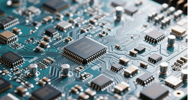
Understanding PCB Assembly
PCB assembly is at the heart of modern electronics manufacturing, involving the meticulous placement and soldering of electronic components onto a printed circuit board. The assembly process demands unmatched precision, as even the slightest misalignment can compromise the performance and reliability of the final product. Surface mount technology (SMT) has revolutionized this field by allowing components to be mounted directly onto the surface of the PCB, rather than relying solely on through-hole methods. This innovation enables higher component density, making it possible to design smaller, more powerful electronic devices that meet the demands of today’s market. Quality control is integral at every stage of PCB assembly, ensuring that each electronic device not only functions as intended but also meets rigorous industry standards. For manufacturers, mastering the assembly process and understanding the nuances of surface mount technology is essential for producing reliable, high-performance printed circuit boards.
Application Fields of 0.25mm Pitch Components
Due to their extremely small size and high density, 0.25mm pitch components are widely used in consumer electronics, medical equipment, communication systems, and other fields. In these industries, high volume production and extremely high quality standards are essential to meet market demands.
They are particularly prevalent in consumer electronics such as smartphones, tablets, cameras, and GPS devices, where these tiny components help achieve product slimness and high performance.
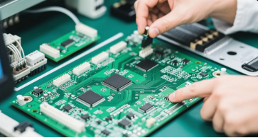
Advanced Equipment and Manufacturing Process
Achieving high precision in PCB assembly relies on a suite of advanced equipment and carefully controlled manufacturing processes. Automated pick-and-place machines are central to the assembly process, enabling the rapid and accurate placement of tiny electronic components onto the PCB. Solder paste is meticulously applied to the solder pads, providing the necessary medium for forming strong electrical connections during the reflow soldering process. Reflow ovens ensure uniform heating, melting the solder paste to create robust solder joints without compromising quality. Inspection systems, such as Automated Optical Inspection (AOI) and X-ray inspection, play a critical role in verifying the integrity of solder joints and detecting any assembly defects. These advanced technologies, combined with precise process control, allow manufacturers to produce high-quality PCB assemblies that meet the stringent requirements of modern electronic devices. The integration of advanced equipment not only improves yield and efficiency but also supports the continuous improvement of the manufacturing process.
Challenges Faced
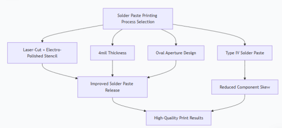
Solder Paste Printing Challenges
For 0.25mm pitch components, solder paste printing requires extremely high precision. Research shows that stencil wiping frequency is the most critical factor affecting print quality.
Laser-cut + electro-polished stencils are typically required, with a thickness generally of 4 mils (about 0.1mm), and oval apertures to ensure good solder paste release. The size and distribution of solder particles in the solder paste also play a crucial role in achieving consistent and accurate prints.
After printing, it is important to remove flux residues to ensure reliable soldering and prevent defects in the final assembly.
Placement Accuracy Challenges
Component placement accuracy requirements are extremely stringent. Studies indicate that an accuracy of ±0.07mm in the Y-direction is necessary for successful 0201 component placement (0201 components measure 0.6mm × 0.3mm).
For even smaller 01005 components (0.4mm × 0.2mm), the accuracy requirements are higher. This means placement machines must possess extremely high mechanical precision and visual recognition capabilities. Advanced vision systems and automated machines are used in these processes to ensure precise alignment and placement of fine-pitch components, supporting the high accuracy needed in modern PCB assembly.
Soldering Process Challenges
Various defects are prone to occur during the soldering process:
·Tombstoning: One end of the component lifts up, usually caused by uneven heating on the two pads.
·Solder Bridging: Short circuits can form during reflow when the pin pitch is too dense and the solder mask design is inadequate.
·Solder Balling: Tiny solder balls can cause short circuits.
Precise temperature control and overall temperature control during the soldering process are critical to prevent these defects and ensure high-quality solder joints. Additionally, wave soldering and selective soldering are used for specific components, providing reliable connections and minimizing defects in complex PCB assemblies.
The Role of Skilled Technicians
While advanced equipment is essential, the expertise of skilled technicians remains a cornerstone of successful PCB assembly. These professionals are responsible for operating and maintaining complex machinery, ensuring that each step of the assembly process is executed with pinpoint accuracy. Skilled technicians possess a deep understanding of both surface mount components and through-hole technology, as well as the intricacies of handling large integrated circuits and a wide variety of electronic components. Their role extends beyond machine operation—they are also tasked with troubleshooting issues, performing quality control checks, and making real-time adjustments to maintain high reliability throughout the assembly line. By combining technical knowledge with hands-on experience, skilled technicians help ensure that every PCB assembly meets the highest standards of quality and performance, supporting the production of advanced electronic devices across industries.
Solutions and Best Practices
1. Optimize Pad Design
For fine-pitch components, pad design requires careful optimization. Symmetrical design of pad thermal capacity can help reduce tombstoning.
2. Precision Solder Paste Printing
Using a stencil with appropriate thickness and aperture design is crucial. For 0.25mm pitch components, Type IV solder paste is generally recommended, as its particle size and distribution better meet the requirements of fine-pitch printing.
3. High-Precision Placement
Investing in high-precision placement equipment is key to successfully assembling 0.25mm pitch components. This equipment should feature:
·High-precision feeders
·Precision component feeding worktables
·High-resolution vision systems
·Advanced component sensors
·A stable base structure to minimize vibration
4. Control Reflow Soldering Process
Optimizing the reflow soldering temperature profile is essential for reducing soldering defects. For fine-pitch components, it is recommended to:
·Use convection reflow with longer soak times
·Employ relatively gentle heating rates
·Control the ramp-up rate to reduce solder balling and tombstoning
5. Refined Stencil Design
A patent application by Huizhou Zecheng Technology Co., Ltd. demonstrates an innovative method: using a specific stencil to apply solder paste precisely at plated through-holes, ensuring connector pins are positioned between solder paste deposits during soldering, thereby reducing pin bending and misalignment.
6. Strict Quality Control
Implementing a multi-level inspection strategy including:
·Automated Optical Inspection (AOI)
·X-Ray inspection (for BGA components)
·In-Circuit Test (ICT)
·Functional Test
Business Impact of Precision Assembly
Precision in the assembly process is not just a technical requirement—it is a key driver of business success in the electronics manufacturing industry. High-precision assembly ensures that electronic devices, from consumer electronics to medical devices and electric vehicles, deliver reliable performance and meet customer expectations. Investing in precision assembly technologies and skilled technicians leads to improved product quality, reduced rework, and higher yields, all of which contribute to a competitive advantage in the marketplace. Conversely, errors or defects in the assembly process can result in costly recalls, reputational damage, and loss of customer trust. By prioritizing precision and continuous improvement, manufacturers can produce complex electronic devices with higher component density and advanced functionality, positioning themselves as leaders in a rapidly evolving industry. Ultimately, the commitment to precision assembly translates into long-term business growth and sustained customer satisfaction.
Future Development Trends
Electronic components continue to trend towards miniaturization. 01005 components (0.4mm × 0.2mm) are already in use. Compared to the PCB area required for 0201 components, 01005 components can save approximately 50% of the space.
This means we will face even smaller component sizes and higher assembly accuracy requirements in the future. As multi layer pcb designs become more complex, maintaining high pcb performance will be critical to ensure reliability and efficiency. Additionally, through hole assembly will continue to play a role in certain applications, even as surface mount technology advances.
Conclusion
PCB assembly of 0.25mm pitch fine-pitch components is a technology fraught with both challenges and opportunities. It requires manufacturers to invest in high-precision equipment, optimize process parameters, and implement strict quality control.
As technology continues to evolve, we can expect electronic devices to become smaller and more powerful, with fine-pitch assembly technology continuing to play a key role in this evolution.
For electronics manufacturing enterprises, mastering fine-pitch component assembly technology is not only about addressing current challenges but also about seizing the high ground in future technology. Only those enterprises that can precisely control every detail will remain unbeaten in the increasingly miniaturized electronic world.
Have you encountered challenges assembling fine-pitch components in your work? Feel free to share your experiences and insights!
FAQs
Q. What is high-precision PCB assembly?
A. It refers to a high-accuracy assembly technology adapted for fine-pitch components (e.g., 0.25mm pitch BGA) and multi-layer high-density PCBs, with a placement error of ≤ ±0.02mm and a solder joint void rate of ≤ 10%. It is used in fields such as medical devices and aerospace.
Q. What are the core differences compared to standard assembly?
A. ① Precision: Standard placement error ≤ ±0.1mm, high-precision ≤ ±0.02mm
② Components: High-precision focuses on components with a pitch below 0.25mm
③ Inspection: Requires AXI (X-ray inspection) + 3D SPI, whereas standard assembly only uses AOI.
Q. How is the placement accuracy of 0.25mm BGA and similar components controlled?
A. The pick-and-place machine’s vision system is calibrated daily (error ≤ 5μm). Type 5/6 solder paste is used with a stencil aperture ratio of "pad diameter × 0.9". The printing speed is 20-30mm/s, and 3D AOI is used for real-time offset inspection after placement.
Q. How much higher is the cost compared to standard assembly?
A. It is 2-5 times higher, mainly due to: high-precision equipment (e.g., pick-and-place machine + AXI ≈ 8 million RMB, standard equipment ≈ 2 million RMB), higher-cost materials (30%-50% more expensive), and specialized labor for process control.
Q. What are the core application industries?
A. Medical (e.g., minimally invasive surgical robots), aerospace (e.g., satellite modules), high-end consumer electronics (e.g., foldable smartphones), and industrial automation (e.g., PLCs).
Author: Jack Wang

