


Mastering HDI PCB Design: Tips and Techniques
Introduction
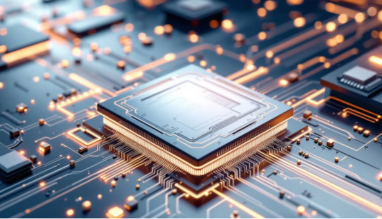
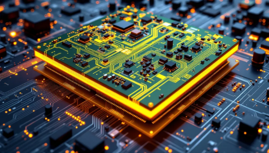
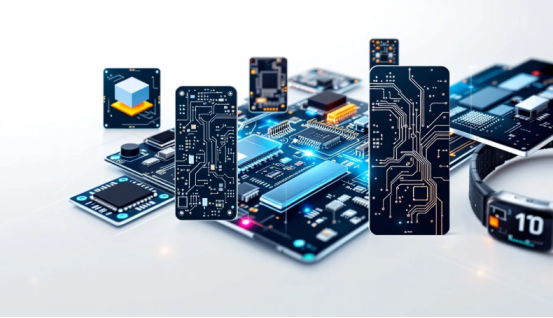
HDI PCBs (High-Density Interconnect Printed Circuit Boards) allow more components in smaller spaces. They use advanced designs for higher density and efficiency in electronic devices. This article covers what HDI PCB technology entails, their benefits, and how to design and manufacture them.
Key Takeaways
·HDI PCBs enable higher wiring density, supporting the miniaturization of electronic devices with advanced design techniques such as via-in-pad technology and careful dielectric material selection.
·Types of vias, including blind, buried, and micro vias, play critical roles in enhancing signal integrity and increasing routing density in HDI PCB designs, despite their manufacturing challenges.
·Understanding design considerations such as aspect ratios, signal routing strategies, and DFM requirements is essential for optimizing HDI PCB performance and manufacturability.
Understanding HDI PCBs
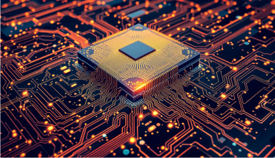
High Density Interconnect (HDI) PCBs represent a leap forward in PCB design, enabling the packing of more capabilities into smaller packages. This is achieved through innovative design techniques that significantly increase higher wiring density compared to standard circuit boards. Imagine fitting an average of 120 to 160 pins per square inch—this is the kind of component density HDI PCBs offer, facilitating the miniaturization of electronic devices. Additionally, the efficiency of pcb assembly plays a crucial role in optimizing the production of these advanced circuit boards.
The implications of this higher pin density are profound. HDI PCBs support the creation of more compact and efficient devices by accommodating more interconnections within smaller physical spaces. Design innovations such as via-in-pad technology further enhance signal integrity by minimizing signal path lengths, ensuring that your devices not only become smaller but also perform better with a reduced layer count.
Moreover, the choice of dielectric thickness materials plays a crucial role in the quality and reliability of these high-density boards.
Benefits of HDI Technology
Adopting HDI technology brings a myriad of benefits, including:
·The ability to achieve a higher density of components per unit area, which is crucial for the ongoing trend of electronic device miniaturization.
·Placing components closer together in HDI circuit boards significantly improves signal integrity.
·Shorter signal paths reduce parasitic effects and enhance performance.
The use of stacked micro vias in HDI PCB design also enhances signal integrity. These vias offer a shorter path for electrical signals, reducing parasitic effects and enhancing overall signal quality. This makes HDI technology indispensable in high-performance applications where signal integrity is paramount.
Types of Vias in HDI PCBs
Vias are the unsung heroes of HDI PCB design, acting as small, copper traces lined holes that facilitate the transfer of electrical signals between different layers of a printed circuit board. Blind, buried, micro vias, and hidden vias are essential in HDI PCBs for increased routing density and enabling smaller board designs.
These vias are particularly crucial in modern device designs, such as smartphones and laptops, where space is at a premium.
Blind Vias
Blind vias showcase remarkable engineering. They link the outer layers to the inner layers without going through the entire board. Commonly used in high-density interconnect and high-speed digital circuits, blind vias enable more compact designs, save valuable space, and improve signal integrity by shortening signal paths. Nonetheless, producing blind or buried vias presents its own challenges, called blind vias. Accurate drilling and plating are crucial, which can raise manufacturing costs.
Despite these challenges, the benefits of blind vias are undeniable. Blind vias offer a solution for linking surface-mounted components without the need for through-hole vias, thereby reducing the risk to prevent solder bridging and enhancing the overall reliability of the circuit board. In essence, blind vias are indispensable for achieving high-performance, space-efficient PCB designs.
Buried Vias
Buried vias are another critical component in HDI PCBs, connecting the inner layer without reaching the outer layers. This unique configuration allows for increased density in PCB designs, as it frees up space on the surface layers for additional components. However, using a buried via comes with its own set of challenges, such as managing larger aspect ratios, which can increase manufacturing costs and complexity. Buried vias connect the inner layers effectively.
To effectively incorporate buried vias into your PCB design, it’s essential to verify the number of buried vias and ensure they do not interfere with other components. This careful planning helps maintain the integrity of the PCB and ensures that the buried vias perform their function without causing any issues.
Micro Vias
Micro vias are the epitome of precision engineering in HDI PCBs. These small holes, typically with a diameter of 150 microns or less, enhance density and signal quality in designs with fewer layers. Primarily used in high-speed digital and RF applications, they are indispensable in devices like smartphones, tablets, and portable electronics.
The manufacturing of micro vias commonly involves laser drilling, a technique that allows for precise depth control and high accuracy in hole placement. This precision is crucial for HDI PCB design, as it ensures that the micro vias are created accurately, enhancing the overall reliability and performance of the board. Furthermore, stacked micro vias facilitate better heat dissipation, creating a network for efficient heat transfer. Additionally, the process to drill vias is essential for optimizing the design.
Micro vias also support enhanced signal integrity by reducing the distance signals must travel, thereby minimizing signal loss and improving overall signal quality. Their contribution to a robust design and enhanced reliability makes them a standard feature in HDI PCBs, enabling the creation of more compact and efficient electronic devices.
The HDI PCB Manufacturing Process
The HDI PCB manufacturing process is a complex and intricate journey that involves specific steps not found in conventional pcb manufacture processes. These steps often include several lamination cycles, integration of complex via structures, and the use of advanced drilling techniques, all of which contribute to the fabrication process of high-performance HDI circuit boards.
Sequential Lamination
Sequential lamination is a cornerstone of HDI PCB manufacturing, allowing for the construction of multilayer PCBs layer by layer. This process involves creating multiple subsets of copper and dielectric layers, which are then bonded together to form the final multilayer PCB with a protective layer applied. The precision required in sequential lamination ensures that each layer aligns perfectly, contributing to the overall reliability and performance of the PCB.
Sequential lamination plays a crucial role in the fabrication of HDI boards by enabling the integration of complex via structures and multiple layers. It allows for the creation of high-density designs without compromising on the quality or performance of the final product through sequential laminations, including the number of layers in a multi layer board and board layers.
Laser Drilling Technology
Laser drilling technology is predominantly used in the creation of microvias in HDI PCBs, providing the precision and control needed for intricate designs. This technology allows for depth-controlled blind vias, ensuring that each hole is drilled to the exact specifications required for optimal performance. Despite its benefits, laser drilling also presents challenges, such as ensuring precise drilling and maintaining quality during the plating process.
The accuracy and precision offered by laser drilling make it an indispensable tool in the HDI PCB manufacturing process. Laser drilling technology ensures the creation of reliable and high-performance HDI circuit boards by overcoming the challenges associated with drilled hole production.
Metalization Techniques
Metalization techniques are crucial in the HDI PCB manufacturing process, with primary methods including chemical etching and plasma via formation. Chemical etching involves using chemicals to remove material and create precise patterns on the PCB, while plasma via formation utilizes plasma to form conductive pathways. These fabrication techniques ensure that the vias in HDI PCBs are void-free and have sufficient wrap plating, which is essential for reliable electrical connections.
Employing these advanced metalization techniques allows manufacturers to create HDI PCBs that meet the high standards required for modern electronic devices. The precision and reliability of these techniques ensure that each via functions as intended, contributing to the overall performance and durability of the PCB.
Design Considerations for HDI PCBs
Designing HDI PCBs requires careful consideration of various factors to maximize performance and reliability, including:
·Managing aspect ratios
·Signal routing strategies
·Understanding DFM (Design for Manufacturability) requirements Each design decision plays a crucial role in the final outcome of the PCB.
Managing Aspect Ratios
Aspect ratios are a critical consideration in via design, as maintaining appropriate ratios ensures the reliability of HDI PCBs. For microvias, adhering to aspect ratio limits is essential to prevent manufacturing issues and ensure long-term reliability. Larger aspect ratios, particularly in blind vias, can lead to increased costs and manufacturing problems, making it crucial to plan the layout carefully.
When designing an HDI PCB, consider factors such as trace width, via size, and the placement of components. These considerations help in optimizing the PCB layout, ensuring that the aspect ratios are maintained within acceptable limits for reliable performance.
Signal Routing Strategies
Effective signal routing is paramount in HDI PCBs to prevent signal reflection and enhance signal quality. Factors that play a role in routing efficiencies include:
·Stackup
·Via architecture
·Parts placement
·Design rules
By managing these factors through thoughtful design, you can achieve higher signal integrity and overall PCB performance with controlled impedance.
Incorporating effective routing strategies ensures that the routing layers and signal paths are optimized, reducing the likelihood of signal degradation. This not only improves signal quality but also enhances the overall reliability and performance of the routing traces signal layer PCB, ultimately improving signal quality.
DFM Requirements
Understanding Design for Manufacturability (DFM) principles is crucial in HDI PCB design to improve yield during manufacturing. DFM checks help identify potential issues before production begins, ensuring a smoother manufacturing process. Incorporating automation in design software can streamline the DFM process, making it easier to adhere to fabricator requirements.
Ensuring that your ECAD software reflects the DFM requirements set by fabricators helps optimize the design for production. This not only improves yield but also reduces the likelihood of manufacturing defects, resulting in a more reliable and high-performance PCB.
Common Applications of HDI PCBs
HDI technology has become essential in various modern applications, including:
·Medical devices: HDI PCBs enable the creation of compact medical devices, such as implants and imaging equipment, which require high performance in small form factors.
·Smartphones: Utilize HDI PCBs with Every Layer Interconnection (ELIC) technology, allowing for thinner and lighter devices.
·Automotive systems: HDI technology is also applied in automotive systems for enhanced performance and compact design.
Wearable technology, such as smartwatches and VR headsets, increasingly depends on printed circuit boards for their compact design. The automotive industry favors HDI PCBs for their small size, which helps integrate advanced electronic features in vehicles.
Additionally, the military and aerospace sectors employ HDI PCBs due to their reliability in extreme conditions and compact size.
Summary
Mastering HDI PCB design requires a deep understanding of various via types, manufacturing processes, and design considerations. Blind, buried, and micro vias each play a vital role in achieving high-density, high-performance PCBs. The manufacturing process, including sequential lamination, laser drilling, and metalization techniques, ensures the creation of reliable HDI circuit boards. Thoughtful design strategies, such as managing aspect ratios and effective signal routing, further enhance PCB performance. As HDI technology continues to evolve, its applications in medical devices, smartphones, automotive systems, and beyond underscore its importance in modern electronics. By leveraging these insights, you can create more compact, efficient, and reliable PCBs that meet the demands of today’s advanced technologies.
FAQs
Q.What are the primary benefits of using HDI PCBs?
A.The primary benefits of using HDI PCBs include higher component density, enhanced signal integrity, and reduced board size, making them especially suitable for compact electronic devices.
Q.How do blind vias differ from buried vias?
A.Blind vias connect outer layers to inner layers without penetrating completely, whereas buried vias are exclusively inter-layer connections that do not reach the outer surfaces.
Q.Why is laser drilling technology important in HDI PCB manufacturing?
A.Laser drilling technology is crucial in HDI PCB manufacturing as it enables the precise and controlled creation of microvias, essential for optimizing high-density, high-performance designs. This specificity enhances the overall functionality and reliability of the printed circuit boards.
Q.What challenges are associated with the use of buried vias?
A.Buried vias often present challenges such as increased production complexity, higher costs, and the necessity for precise alignment during fabrication. These factors can significantly impact manufacturing efficiency and overall project timelines.
Q.What are some common applications of HDI PCBs?
A.HDI PCBs are essential in medical devices, smartphones, wearable technology, automotive systems, and military/aerospace applications due to their compact size and high performance. These applications highlight the versatility and efficiency that HDI technology offers across various industries.
Author: Jack Wang

