


Essential Guide to Effective PCB Design: Tips and Techniques
Introduction
"A well-designed PCB is like a precision-engineered city—components are the buildings, traces are the roads, grounding is the foundation, and noise immunity is the defense system."
Whether you're an electronics enthusiast or a professional engineer, mastering the core principles of PCB design can transform your circuits from "functional" to "exceptional." This article breaks down key principles and techniques in accessible language, helping you avoid 90% of common pitfalls in practical design.
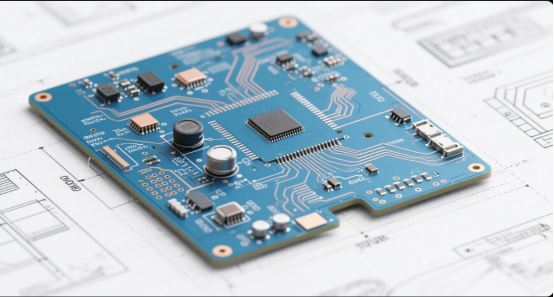
What is PCB and Why Does It Matter?
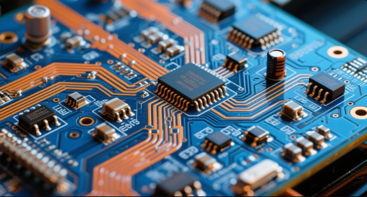
PCB (Printed Circuit Board) serves as the central skeleton and neural network of electronic devices. It provides both physical support for electronic components and interconnects them through precisely arranged conductive pathways to form complete circuit systems.
In today’s electronic world, PCBs play an indispensable role—from small embedded systems to large data center equipment. A well-designed PCB significantly enhances circuit reliability, stability, and noise immunity, while a poorly designed one can cause complete system failure. PCB design choices are especially critical for applications operating in harsh environments, such as military or medical fields, where reliability is paramount.
Fundamental Steps in PCB Design
PCB design is a systematic engineering process that typically involves these six fundamental steps:
·Requirements Analysis: Define functional requirements, size constraints, and operating environment. Accuracy at this stage directly affects subsequent design effectiveness.
·Schematic Design: Use EDA software to draw circuit schematics, utilizing schematic capture as the process of creating a schematic diagram, which serves as the logical representation of the circuit and is the foundation for schematic creation. Incorporate schematic symbols to represent components and ensure that accurate design data is generated during schematic capture for manufacturing.
·Layout Planning: Arrange component placement based on the schematic, using a CAD tool or design tool to place components and define the board shape. Consider the position of component pins and net connections for optimal connecting components, signal integrity, power distribution, and thermal management.
·Routing: Route traces while ensuring electrical performance, paying attention to signal path direction, trace width, and via usage between layers. PCB routing is the process of connecting component pins according to the schematic and adhering to pcb design rules.
·Verification Check: Use DRC (Design Rule Check) tools to validate the design and ensure compliance with all pcb design rules, checking that the board design meets all logical and physical requirements.
·Manufacturing File Generation: Output files for PCB manufacturing, such as Gerber files and drill files. These are manufacturing files generated from the design data, which are essential for accurate fabrication.
The entire board design process is facilitated by advanced CAD tools and design tools, which help manage net connections, component placement, and the transition from schematic capture to manufacturing files.
Ten Golden Rules of PCB Design
Board Material Selection: Materials Determine Longevity
FR-4 remains the preferred material for general applications, balancing cost and heat resistance. FR-4 is a type of rigid substrate commonly used in the vast majority of printed circuit boards, providing a stable and high-temperature-resistant base for copper traces and component placement.
For RF or high-speed signals (>500MHz), Polytetrafluoroethylene (PTFE) substrates can reduce signal loss. After fabrication, the result is a bare board, which serves as the foundation for component assembly.
Dimension Design: Balancing Space and Performance
Maintain 2-5mm clearance from enclosure dimensions to avoid assembly conflicts. Increase copper thickness (e.g., 2oz) in high-power areas and provide thermal relief channels.
Component Placement: Zoning is Key
Place analog circuits (op-amps, ADCs) and digital circuits (MCUs, FPGAs) in separate zones with ≥5mm spacing. Position high-current devices close to power sources to reduce voltage drop along power paths. When you place components, such as integrated circuits and through hole components, consider their orientation and proximity to related parts to optimize performance, manufacturability, and ease of assembly.
Layout should follow the “big-to-small, difficult-to-easy” principle—prioritize placing critical unit circuits and core components first.
The Art of Routing: 3W Rule and Serpentine Traces
Maintain trace width ≥8mil for regular signals and ≥15mil for high-voltage lines; keep adjacent trace spacing ≥3 times the trace width (3W rule). For high-speed signals (e.g., DDR), maintain strict length matching for differential pairs with ≤5mil tolerance. In multi-layer PCB designs, pcb routing becomes more complex and often requires extra layers and careful pcb stack up planning to ensure optimal electrical performance and mechanical integrity.
Avoid 90-degree bends to reduce signal reflection; maintain appropriate trace spacing to minimize crosstalk. Using a dedicated ground plane during pcb routing can further improve signal integrity and reduce electromagnetic interference.
Grounding Strategies: Single-point vs. Multi-point
Use "star" single-point grounding for analog circuits to prevent ground loops. Implement large-area copper pours for low-impedance grounding in high-frequency digital circuits.
Proper grounding design is fundamental to circuit stability—ensure every circuit section has effective grounding to reduce noise and improve signal integrity.
Three Anti-Interference Techniques
Install metal shields over RF modules or crystals; place decoupling capacitors (0.1μF ceramic + 10μF tantalum) near chip power pins; surround critical signal traces with grounding vias to create "Faraday cages."
Pad Design: Details Determine Reliability
SMD pads should be 0.2-0.5mm wider than component leads to prevent cold joints. Through-hole pads should have ≥25μm copper wall thickness to avoid copper layer fracture under high temperatures.
Large-Area Filling: Beyond Aesthetics
Fill unused areas with copper connected to ground to reduce impedance. Avoid isolated copper islands that can act as antennas—connect them to ground using vias.
Jumper Wires: The Last Resort
Use jumpers only for debugging—strictly prohibit them in production boards. Single-layer boards may use 0Ω resistors as jumpers instead.
High-Frequency Routing: Need for Speed
Control impedance (e.g., 50Ω) for surface-layer high-frequency signal traces—calculate dielectric thickness precisely. Avoid 90° bends; use 45° angles or arc transitions to reduce signal reflection.
Designing for Manufacturability
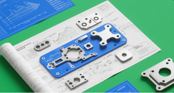
Designing for manufacturability is a vital step in the printed circuit board (PCB) design process that ensures your ideas can be efficiently transformed into a reliable final product. By considering manufacturability from the outset, you can avoid costly redesigns and production delays. This means thinking ahead about how your PCB layout, component placement, copper traces, and electrical connections will translate from digital design to physical circuit board. A manufacturable design not only streamlines the production process but also enhances the quality and consistency of your printed circuit boards, making sure your board performs as intended in real-world applications.
Optimizing Layout for Production
A well-optimized layout is the backbone of a smooth manufacturing process. Strategic component placement can make automated assembly faster and more accurate, reducing the risk of placement errors. When arranging components, keep similar parts aligned and oriented in the same direction to simplify assembly. Minimize the number of drill holes and vias, as each additional hole increases production time and cost. Carefully define the board outline to ensure compatibility with standard manufacturing panels and equipment. By focusing on these layout details, you can create a board that is not only easier to produce but also more reliable and cost-effective.
Material and Process Constraints
Every PCB is built from a combination of copper layers, insulating material, and protective coatings like solder mask. Understanding the properties and limitations of these materials is essential for a successful design. For example, the thickness of the copper layer affects current-carrying capacity, while the choice of insulating material impacts signal integrity and thermal performance. The solder mask protects copper traces from oxidation and helps prevent solder bridges during assembly. Additionally, the manufacturing process—such as etching, drilling, and soldering—imposes its own set of constraints. By designing with these factors in mind, you can create a board that is well-suited to the chosen materials and processes, reducing the risk of defects and ensuring a smoother transition from design to production.
Cost-Effective Design Choices
Balancing performance and cost is a hallmark of good PCB design. Making cost-effective choices starts with simplifying the board layout wherever possible—reducing unnecessary complexity can lower both material and assembly costs. Selecting standard components and consolidating similar parts can also help keep expenses in check. Opt for low-cost materials that still meet the performance requirements of your final product, and avoid over-specifying features that add little value. By making smart decisions throughout the design process, you can deliver a high-quality board that meets both technical and budgetary goals.
Complex Designs: Scaling Up Your PCB Projects
As electronic devices become more sophisticated, the demands placed on printed circuit board (PCB) designs grow as well. Modern circuit boards must handle higher speeds, greater component density, and increased reliability requirements. Scaling up your PCB projects means addressing challenges like maintaining signal integrity, ensuring robust power distribution, and managing heat dissipation—all while fitting everything into a compact board. By leveraging advanced design techniques and tools, you can create printed circuits that meet the needs of today’s high-performance electronic devices.
Multi-Layer Boards
Multi-layer boards are essential for tackling the complexity of advanced PCB projects. By stacking alternating layers of copper traces and insulating material, designers can dramatically increase the number of electrical connections and components that fit on a single board. This approach not only boosts circuit density but also improves signal integrity and reduces electromagnetic interference, which is critical for high-speed applications. However, designing multi-layer PCBs introduces new challenges, such as carefully planning the stack up to control impedance and manage thermal expansion. Using powerful PCB designing software like Altium Designer allows you to create and simulate complex multi-layer boards, ensuring that your design meets all performance and reliability requirements. With the right tools and techniques, you can confidently scale your projects to meet the demands of the modern electronics industry.
Popular PCB Design Software Options
Choosing the right tools is half the battle: PCB designers select software based on the requirements of their projects, such as designing for IoT devices or high-speed applications.
·Altium Designer: Powerful professional-grade PCB design software suitable for complex circuits, offering complete solutions from schematic to PCB layout.
·Eagle: User-friendly PCB design software ideal for beginners and small projects, featuring an intuitive interface and extensive component libraries.
·KiCad: Open-source PCB design software with strong community support, suitable for beginners and intermediate users, with continuously improving features.
·Cadence Allegro: Enterprise-level PCB design solution for high-speed, high-density circuits, widely used in large corporations.
Learning and Practice Recommendations for PCB Design
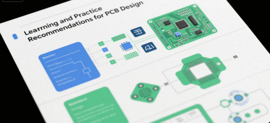
PCB design is a process of continuous learning and practice. Staying updated with the latest design trends and technologies, participating in relevant forums and communities, and exchanging experiences with other designers are effective ways to improve your skills.
For beginners, start with a simple project (e.g., an LED flasher circuit) and follow the complete workflow from schematic to layout and routing to gain practical experience. This includes creating both the schematic and the PCB layout, as well as learning how to generate outputs such as silk screen layers for component identification. Additionally, learning to use simulation tools for signal and power integrity analysis can help identify and resolve potential issues before manufacturing.
Participating in open-source hardware projects or online design communities can provide valuable feedback and suggestions. Many experienced engineers are willing to share their knowledge and techniques, which can significantly accelerate your learning curve.
Conclusion
PCB design is an art and science combining electronics, mechanical engineering, and materials science. With the trend toward miniaturization and higher performance in electronic products, PCB design faces increasing challenges. Mastering fundamental design principles and techniques not only improves design efficiency but also enhances product reliability.
Remember: excellent PCB design requires finding the balance between functionality, reliability, manufacturing cost, and producibility. By following the ten golden rules outlined in this article and engaging in continuous practice, you'll be able to design superior, more reliable PCB circuit boards.
As a seasoned engineer aptly noted: "There's no single best solution in PCB design—only the most appropriate solution for the specific application." In practical design, apply these principles and techniques flexibly based on concrete scenarios and requirements. Continuous learning and accumulated experience remain indispensable on the path to becoming an exceptional PCB designer.
FAQs
Q: How should the chip filtering capacitor be placed in PCB design?
A: The filtering capacitor should be placed as close as possible to the chip pins.
Q: What is the relationship between PCB trace width and current?
A: Generally, the larger the current, the wider the required trace width. Specific values can be determined using relevant formulas or empirical tables.
Q: How are analog ground and digital ground allocated in PCB design?
A: Typically, the two are isolated and connected using a single-point grounding approach.
Q: What is a Gerber file, and why is it important?
A: Gerber files contain all the information required for PCB manufacturing, such as copper layers, solder mask layers, silkscreen layers, etc. Manufacturers use these files to produce PCBs, making the generation of accurate and high-quality Gerber files a critical step.
Q: How to avoid high-frequency interference?
A: The basic approach is to reduce the electromagnetic field interference of high-frequency signals. This can be achieved by increasing the spacing between high-speed signals and analog signals, or adding ground protection or shunt paths next to analog signals. Additionally, attention should be paid to the noise interference from digital ground to analog ground.
Q: Why shouldn’t vias be drilled on solder pads of surface-mounted components?
A: Drilling vias may affect soldering quality, leading to weak soldering or short circuits, and may also impact the electrical performance and mechanical stability of the components.
Q.Signal Integrity Issues
A.Improve signal quality by adding termination resistors and optimizing trace geometry. For high-speed signals, pay attention to impedance matching and signal reflection issues.
Q.Electromagnetic Compatibility (EMC) Issues
A.Reduce electromagnetic interference (EMI) and susceptibility through shielding, filters, and rational layout planning. Keep critical signal traces away from board edges and interface areas.
Q.Thermal Management Issues
A.Improve heat dissipation through rational placement of heat-generating components and auxiliary cooling facilities like heat sinks and fans. Distribute heat-generating components evenly to facilitate board and system cooling—keep temperature-sensitive devices away from high-heat components.
Author: Jack Wang

