


Understanding the PCB Layer Key Insights for Designers and Engineers
Introduction
Meta Description: Struggling to choose PCB layers for your design? This in-depth guide breaks down the basics of PCB stack-up, from single-sided to complex multilayer boards. Learn the function of signal, power, and ground planes, and how to choose the right layer count for performance, cost, and reliability.
Introduction: It’s More Than Just a “Sheet”
Inside every electronic device—your phone, laptop, or smartwatch—lies a green circuit board, the PCB. The PCB forms the backbone of the electronic circuit within modern devices, providing the essential wiring and component arrangement. You might have heard terms like “4-layer” or “6-layer board,” but have you ever wondered why these thin boards are built in layers? PCB layers are like sheet layers—the foundational building blocks of the board, much like the layers of a house’s foundation, laminated from copper sheets on non-conductive substrates. Does more layers always mean better?
Choosing the wrong number of layers can lead to signal interference, unstable power delivery, poor heat dissipation, and even force a complete project redesign. Let’s take a deep dive into the world of PCB layers. We’ll skip the confusing jargon and explain everything in plain English.
The Basics: What Exactly Are Printed Circuit Board Layers?
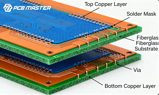
Think of a PCB as a super-compact, multi-layered sandwich. It’s far more than just a board with lines on it.
A standard PCB is made up of these different layer types:
·Signal Layers: These are the board’s “nervous system.” Made of etched copper foil, they carry electrical signals between components. These layers are often formed by a thin layer of conductive material, typically copper, laminated onto the substrate. When we say “4-layer” or “6-layer” board, we’re primarily counting the signal layers.
·Power Plane: A dedicated, solid copper layer used for distributing power. It acts like the “circulatory system,” delivering stable “nourishment” (electrical power) to all chips and components. These layers act as dedicated reference planes for power distribution.
·Ground Plane (GND Plane): Another solid copper layer that acts as a common reference point for the circuit. It’s the “return path” for signals, a “shield” against external interference, and also helps with heat dissipation. These layers act as essential reference planes for signal return.
·Silkscreen Layer: The white text and symbols printed on the board. It’s the “instruction manual” for engineers and technicians, showing component placement, values, and orientation. Silkscreen layers are crucial for adding text designators, labels, and identifiers, aiding in troubleshooting, branding, and documentation.
·Solder Mask Layer: The familiar green (or other color) coating. It prevents solder bridges during assembly and protects the copper traces from oxidation and damage. Solder masks are protective coatings applied to the surface copper layers to prevent short circuits and protect traces.
The substrate layer forms the foundation of the PCB, providing mechanical support and electrical insulation for the entire board structure.
So, when discussing how many layers a PCB needs, we’re really talking about the arrangement of signal layers, power planes, and ground planes.
Between the copper layers, there are insulating materials known as dielectric materials. The dielectric constant of these materials affects signal propagation speed and impedance control, which is especially important in high-speed PCB designs. These insulating and dielectric materials are critical for maintaining electrical insulation, signal integrity, and thermal management within complex layered PCB structures.
From Simple to Complex: A Detailed Look at Common PCB Layer Stack-ups
1. Single-Sided Boards
·Structure: Only one conductive copper layer, which serves as the only conductive layer for signal routing. All traces are routed on that single layer. Components are on one side, traces on the other.
·Pros: Lowest cost, simplest to manufacture, fastest turnaround.
·Cons: Extremely limited routing space, unsuitable for complex circuits. Traces can’t cross, requiring “jumper wires” if routes intersect.
·Use Cases: Very simple electronics like basic toys, low-end radios, electronic doorbells, or control circuits in household appliances and simple industrial systems. Rare in modern, complex devices.
2. Double-Sided Board
·Structure: In double layer PCBs, components and traces can be mounted on one or both sides, providing greater design flexibility. Both the top and bottom layers are used for signal routing, with the bottom layer serving as an additional routing and mounting surface. The two layers are connected by vias (plated-through holes).
·Pros: Still very low cost, offers twice the routing area of a single-sided board. The most common and versatile choice for simple designs.
·Cons: Can still be insufficient for complex MCU/CPU circuits. Requires more careful consideration for signal integrity.
·Use Cases: Arduino boards, simple controllers, appliance motherboards, smart toys. Double layer PCBs are commonly used in applications requiring surface mount components for increased density. The go-to choice for hobbyists and simple products.
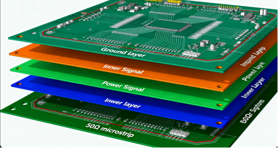
3. 4-Layer Boards – The Value Leap
This is the crucial step from “simple” to “professional.” A typical four layer board stack-up is: Top (Signal Routing Layer) -> Inner Layer 1 (Ground Plane) -> Inner Layer 2 (Power Plane) -> Bottom (Signal Routing Layer)
·Pros:
·Dedicated Power/Ground Planes: Provide extremely stable, low-noise power, greatly improving noise immunity.
·Improved Signal Integrity (SI): High-speed signals can be routed adjacent to a ground plane, providing a clear return path and reducing electromagnetic interference (EMI).
·Better Routing Freedom: The addition of extra signal layers, such as two extra signal layers in a four layer board, allows for more complex routing layers and improved circuit density, especially when using blind/buried vias.
·Use Cases: Most ARM/MCU-based products, industrial control boards, smart home hubs, advanced consumer electronics. Higher pin density in modern components often necessitates the use of four layer boards to ensure proper signal routing. The best balance of performance and cost.
4. 6-Layer Boards & Beyond – The High-Performance Arena
Six or more layers are common in advanced multilayer PCBs for high-performance applications. Needed for higher-speed circuits (>100MHz), complex interfaces (DDR memory, high-speed USB, HDMI), and high component density.
·Typical 6-Layer Stack-up: Top (Sig) -> L2 (GND) -> L3 (Sig) -> L4 (Sig) -> L5 (PWR) -> Bottom (Sig). In multilayer PCBs, an entire layer can be dedicated to ground layers or power connections, which improves signal integrity and EMI management.
·This provides more signal layers while ensuring each is adjacent to a reference plane (power or ground).
·8, 10, 12-Layer Boards: Introduce more signal layers and dedicated planes. Higher component density is achieved through the use of additional internal layers and advanced routing techniques. They can use stripline routing (signals embedded between two planes) for critical signals, offering superior shielding.
·Pros:
Excellent Signal Integrity (SI) and Power Integrity (PI).
Strong immunity to EMI and reduced emissions.
Capable of handling highly complex routing and high-density layouts.
Support for transmission lines, such as microstrip and stripline, for high-frequency signal routing in multilayer PCBs.
·Use Cases: Smartphones, high-end GPUs, server motherboards, network routers, communication equipment.
Why Are More Layers Better? Key Advantages
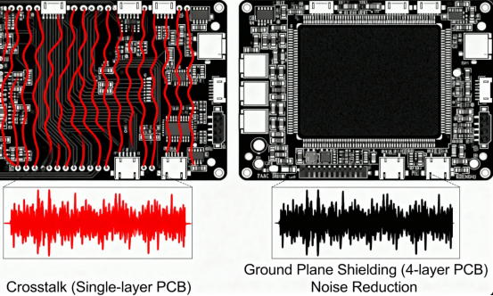
·Guardian of Signal Integrity (SI): High-speed signals are sensitive. More layers allow every critical trace to be placed next to a continuous reference plane (usually ground), ensuring clean signals and preventing noise-related errors. Careful design of signal traces is essential for maintaining signal quality, especially in high-speed multilayer boards. This is crucial for stability and reliability.
·Backbone of Power Integrity (PI): A dedicated power plane acts like a reservoir, instantly responding to a chip’s current demands, preventing voltage dips and system crashes. More layers often mean lower impedance in the power distribution network (PDN).
·Ultimate Shield for EMC: Solid ground and power planes are natural EMI shields. They contain noise within the board and protect it from external interference. This is key to passing stringent EMC certifications (CE, FCC).
·Routing Freedom & Space Saving: More layers mean wider “highways” for traces. This allows for reduced via count and optimized layout, potentially shrinking the PCB size and lowering overall assembly cost. Increasing board thickness can improve heat dissipation, but it must be balanced with design and inspection requirements.
Power Distribution: Ensuring Reliable Performance Across Layers
·Power distribution is the backbone of any printed circuit board, especially as designs move from simple two-layer boards to complex multi layer PCBs. In these advanced boards, power planes—dedicated layers of copper—are strategically placed within the inner layers, while the outer layers typically handle signal routing and component placement. This separation not only streamlines the delivery of power to every electronic component but also plays a crucial role in minimizing electromagnetic interference and maintaining signal integrity.
·A well-designed power distribution system in a multi layer PCB uses thick copper planes to provide low impedance paths for power supplies, ensuring that voltage drops are minimized even under heavy load. The connection between power planes and components is achieved through vias that pass through the insulating layers, allowing current to flow efficiently from the inner layers to the board surface.
·Engineers often employ multiple power planes within the PCB layer stack to support different voltage domains or to handle higher current demands. Careful selection of copper thickness, trace width, and via size is essential to reduce resistance and power losses. Additionally, the use of decoupling capacitors near power pins helps filter out noise, further stabilizing the power delivered to sensitive integrated circuits.
·Optimizing the layout of power planes and signal layers, and ensuring that power and ground planes are placed adjacent to each other, can significantly reduce EMI and improve overall circuit board performance. By focusing on these design principles, engineers can create printed circuit boards that deliver reliable, efficient power across all layers, supporting even the most demanding electronic applications.
How to Choose the Right Number of Layers for Your Project
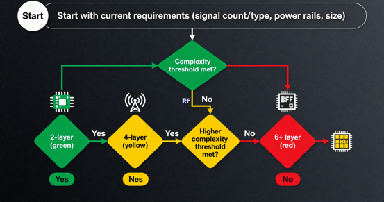
This is a balancing act. Follow this decision process:
1.Assess Circuit Complexity:
·Simple logic, low frequency (< 10MHz): A 2-layer board is likely sufficient.
·MCU (e.g., STM32), common peripherals (SPI, I2C), medium frequency: A 4-layer board is the safest, most professional choice. It prevents many potential issues.
·Processor (e.g., ARM Cortex-A), DDR memory, high-speed interfaces (USB, MIPI), RF circuits: Requires at least 6 layers, often 8 or more.
2.Consider Cost:
·Layer count is a primary cost driver. Each added pair of layers increases cost significantly.
·The Balance: Ask yourself: “Am I willing to risk 50% more debugging time, potential failure, and instability to save 10% on PCB cost?” Often, choosing one more layer than the “bare minimum” is the wiser investment.
3.Consider Physical Size and Density
·If the product is tiny (e.g., wearables) but feature-rich, you must increase layers to get enough routing space.
4.Consult Your PCB Manufacturer:
·Before finalizing, send your draft design and requirements to your PCB fab’s engineer. Their experience is invaluable for recommending the most cost-effective stack-up.
·Discuss substrate material options with your manufacturer, as the choice of substrate material (such as FR-4 or polyimide) directly affects the electrical, thermal, and mechanical properties of your PCB.
Manufacturing Considerations: Turning Your Design into Reality
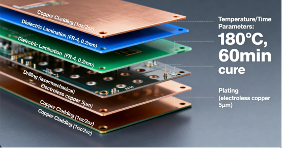
·Transforming a PCB design from digital layout to a physical circuit board involves a series of precise manufacturing steps. Each stage—fabrication, assembly, and testing—requires careful attention to detail to ensure that the final product meets both functional and quality standards.
·During fabrication, the various PCB layers are created using processes like photolithography and etching, which define the intricate copper traces and planes on each layer. These layers are then bonded together, with insulating substrate materials separating the conductive copper layers. Drilling is used to create holes for vias and component leads, connecting the different layers and enabling complex routing in multi layer PCBs.
·Assembly involves placing and soldering electronic components onto the board surface, with strict tolerances for component placement and orientation to ensure reliable operation. Automated pick-and-place machines and reflow ovens are commonly used to achieve high precision and repeatability.
·Testing is the final step, where the assembled printed circuit board PCB is checked for electrical continuity, shorts, and correct functionality. Design for manufacturability (DFM) principles—such as specifying appropriate clearances, tolerances, and test points—help streamline the manufacturing process and reduce the risk of defects.
·By considering these manufacturing aspects early in the design process, engineers can ensure that their PCB layers are not only optimized for performance but also for efficient, cost-effective production.
Conclusion: The Best Layer Count is the One That's Right for You
Choosing PCB layers is a careful dance between performance, cost, and reliability. There's no single right answer, but there is a core principle: Don't sacrifice hidden stability and performance for obvious cost savings.
For most embedded development and electronic products, a 4-layer board is the "gold standard" starting point. It provides stable power, a clean ground, and sufficient routing space, saving you from countless debugging headaches.
When your design pushes into high-speed, high-density territory, confidently embrace 6, 8, or more layers. They will be the foundation that allows your product to excel in a competitive market.
We hope this guide has helped demystify PCB layers and helps you make the best decision for your next great project!
(Interactive Section)
What layer count does your project use? Any interesting or painful experiences choosing? Share your stories in the comments below!
FAQs
Q: Do more layers always guarantee better performance?
A: Not necessarily. A poorly designed 6-layer stack-up (e.g., signals far from a reference plane) can perform worse than a well-designed 4-layer board. Layers provide potential; good design unlocks it.
Q: Can I port a 2-layer design directly to a 4-layer board?
A: You can, but it's not recommended to just copy-paste. Best practice is to re-optimize the layout. Place critical signals next to the ground plane and ensure all high-speed signals have a solid reference path.
Q: What is HDI? How does it relate to layer count?
A: HDI (High-Density Interconnect) is a technology using smaller microvias, finer traces, and closer spacing to achieve extreme routing density. HDI boards are usually multilayer (6+ layers), but the technology allows achieving similar functionality with fewer layers, or greater complexity with the same layer count. Common in smartphones and ultra-thin laptops.
Q. What are the common standard thicknesses for PCBs?
A. The standard thickness is predominantly 1.6mm (used in approximately 80% of consumer/desktop devices), 2.4mm (for industrial/automotive applications requiring vibration resistance), and 3.2mm (for servers/medical equipment supporting high-power components). Thinner options such as 0.8mm/1.0mm are also available for portable devices.
Q. Does PCB thickness affect heat dissipation?
A. Yes. Thicker boards (e.g., 2.4mm and above) can accommodate heavier copper layers (such as 2oz), improving heat dissipation efficiency by 30%–40% compared to 1.6mm thin boards. This makes them suitable for high-power components like power modules.
Q. What are the limitations of using thin PCBs (below 0.8mm)?
A. Thin PCBs have lower mechanical strength, making them unsuitable for heavy components (e.g., connectors weighing >5g). Additionally, copper thickness must be limited to 1oz or less to prevent cracking during bending. They are commonly used in wearable devices.
Q. How does PCB thickness relate to cost?
A. For every 0.5mm increase in thickness, costs typically rise by 10%–20%. This is due to the need for more substrate and copper, as well as increased complexity in drilling and lamination processes, which result in lower production yield.
Author: Jack Wang

