


High-Speed PCB vs. High-Frequency PCB: Key Differences Explained by PCBMASTER
High-Speed and High-Frequency PCBs: Different Goals, Same System
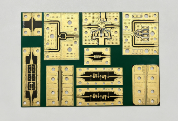
High-speed PCBs and high-frequency PCBs may sound similar, but they are not the same. They have different design goals, performance requirements, and application scenarios. Yet in many modern electronic systems — such as 5G base stations — you often need both at the same time. PCBMASTER provides solutions that precisely meet these single or combined needs, covering everything from pure high-speed digital boards to pure high-frequency RF designs.
4 Key Differences Between High-Speed and High-Frequency PCBs
| Comparison Dimension | High-Speed PCB | High-Frequency PCB |
|---|---|---|
| Core Definition | Transmitting high-speed digital signals (typically ≥1 Gbps, such as DDR5 or PCIe 5.0), with a focus on data transfer rate. | Transmit high-frequency RF or microwave signals (typically ≥1 GHz, such as 5G RF or radar waves), focusing on the signal frequency level. |
| Core Design Goals | Solving Digital Signal Integrity (SI) and Timing Issues: Control Crosstalk, Jitter, and Timing Skew to Ensure Error-Free Data Transmission | Solving RF Signal Loss and Stability Issues: Control Attenuation, Phase Shift, and Radiation to Ensure Distortion-Free, Low-Loss Transmission |
| Key Parameters to Consider | · Differential impedance (e.g., 100 Ω ±10%) · Signal length mismatch (≤ 20 mil) · Jitter (≤ 10 ps) · Crosstalk (≤ -30 dB) | · Characteristic Impedance: 50 Ω ± 5% · Dielectric Loss (Df): ≤ 0.005 · Insertion Loss (S21): ≥ -0.5 dB @ 10 GHz · Phase Stability |
| Typical Applications | Server motherboards, PCIe graphics cards, DDR memory modules, and USB 4.0 devices (pure digital transmission scenarios) | 5G Base Station RF Boards, Radar Antenna Boards, Satellite Communication Modules, and RF Front-End Modules (Pure RF / Microwave Applications) |
3 Shared Features Between High-Speed and High-Frequency PCBs Explained
Because they share many technical similarities, the two are often mentioned together, and PCBMASTER also applies similar core technology solutions in its R&D.
1. Consistent Base Material Selection
Both types require low-loss, highly stable materials. High-speed PCBs typically use modified FR-4 (Df≈0.008) or Rogers RO4000 (Df≈0.0027), while high-frequency PCBs use PTFE (Df≈0.0002) or RO4000. The core goal for both is to reduce signal loss by using materials with low Dk/Df.
2. Similar Process Precision Requirements
Both require micron-level control: line width tolerance within ±5 μm, blind/buried via diameters ≤0.1 mm, and surface finish preferably ENIG. Each batch also needs TDR impedance testing. PCBMASTER’s high-precision production lines can meet the process requirements for both high-speed and high-frequency PCBs.
3. Overlapping EMC and Thermal Management Needs
High-speed signals with fast edges generate high-frequency harmonics (for example, a 10 Gbps signal can produce harmonics up to 50 GHz), while high-frequency signals themselves are strong radiators. Therefore, both types need complete plane, shielding design, and thick-copper heat management. PCBMASTER’s integrated EMC and thermal solutions can handle both challenges simultaneously.
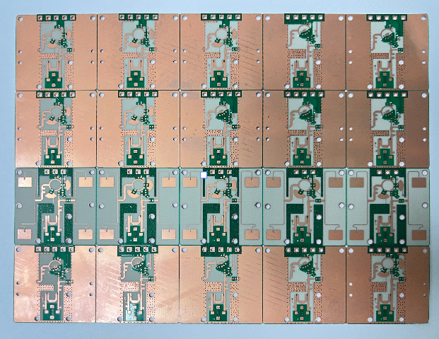
PCBMASTER’s Scenario-Based Solutions for High-Speed and High-Frequency PCBs
| Scenario Type | Technical Focus | Recommended Solution |
|---|---|---|
| Pure High-Speed Digital Applications (e.g., Servers) | Timing Matching, Differential Pair Control, and Low Crosstalk | 12–20 Layer Stackups, Modified FR-4/RO4000 Materials, Fly-By Topology Routing |
| Pure High-Frequency RF Applications (e.g., Radar) | Low Loss, Phase-Stable, High EMC Performance | More than 8 layers, PTFE/RO4000 substrates, shielded cavity design, and full-band impedance control |
| High-Speed + High-Frequency Combined Scenarios (e.g., 5G Base Stations) | Cross-Domain Signal Isolation While Balancing Timing and Signal Loss | Hybrid Laminates (PTFE for RF zones, RO4000 for digital zones) with Partitioned Shielding Design |
Conclusion
High-speed and high-frequency PCBs may have different goals, but modern electronic systems often need both to work together flawlessly. By understanding their key differences, shared features, and applying scenario-based solutions, engineers can achieve reliable, high-performance, and low-loss designs. PCBMASTER’s expertise in materials, precision manufacturing, and integrated EMC/thermal solutions ensures that your boards perform optimally, whether in pure digital, pure RF, or combined high-end applications.
FAQs
1. How does signal crosstalk affect high-speed PCB performance, and how can it be reduced?
Signal crosstalk happens when an electrical signal in one trace interferes with a nearby trace. In high-speed PCBs, this can cause data errors, jitter, or timing issues, especially with differential pairs. To reduce crosstalk, engineers can:
l Increase spacing between critical traces.
l Use ground planes or guard traces to shield signals.
l Arrange differential pairs carefully with controlled impedance.
l Optimize layer stackups so sensitive signals are sandwiched between ground layers.
These methods ensure that high-speed signals stay clean, reliable, and error-free.
2. Why is thermal management critical in combined high-speed and high-frequency PCB designs?
High-speed digital circuits and high-frequency RF circuits generate heat differently. High-speed signals with fast edges create high-frequency harmonics, while high-frequency RF circuits may radiate energy that heats surrounding components. Poor thermal management can cause:
l Component overheating, leading to failures or reduced lifespan.
l Signal drift due to temperature-dependent material changes.
l Increased EMI from hotspots affecting nearby circuits.
To manage heat, designers use thick copper layers, thermal vias, heat sinks, and careful component placement. Effective thermal management ensures long-term reliability and stable signal performance.
3. What are the key challenges when designing a hybrid PCB for both high-speed and high-frequency signals?
Designing a hybrid PCB that handles both high-speed digital and high-frequency RF signals is challenging because the requirements can conflict:
l High-speed signals need tight timing control and low jitter.
l High-frequency RF signals require low loss, phase stability, and shielding.
l Signal interference between domains can degrade performance.
Engineers solve these challenges by:
l Using hybrid laminates, e.g., PTFE for RF zones and RO4000 for digital zones.
l Implementing partitioned shielding and isolated ground planes.
l Carefully planning trace routing, layer stackups, and impedance control for each domain.
This approach ensures both types of signals perform optimally without compromising each other.

