


Engineering Guide to Aluminum Oxide Ceramic-Based PCBs Material, Process, and Application Insights
As electronic devices evolve toward higher power density, greater integration, and stricter reliability demands, the thermal limitations of traditional FR4 substrates have become increasingly evident. Aluminum oxide ceramic-based PCBs, with a thermal conductivity of 25–32 W/m·K (over 100 times that of FR4), a dielectric constant of 9.2–9.8, and a coefficient of thermal expansion (CTE) of 8.1×10⁻⁶/℃ (closely matching silicon chips), offer a core solution to power electronics cooling challenges. Field data from applications in new energy vehicles, 5G base stations, and aerospace show they reduce component operating temperatures by over 40% while enduring more than 1,000 thermal cycles (-40℃ to 125℃).

Ⅱ. In-Depth Material Performance Analysis
1. Grading and Selection of Aluminum Oxide Ceramics
· 96% Alumina: A cost-effective choice with 25 W/m·K thermal conductivity and 18 kV/mm dielectric strength, suitable for medium-power LED lighting and industrial control modules.
· 99.5% Alumina: A high-performance variant with 32 W/m·K thermal conductivity and 395 MPa flexural strength, capable of long-term operation at 150℃, ideal for IGBT modules in new energy vehicles.
2. Key Performance Parameter Comparison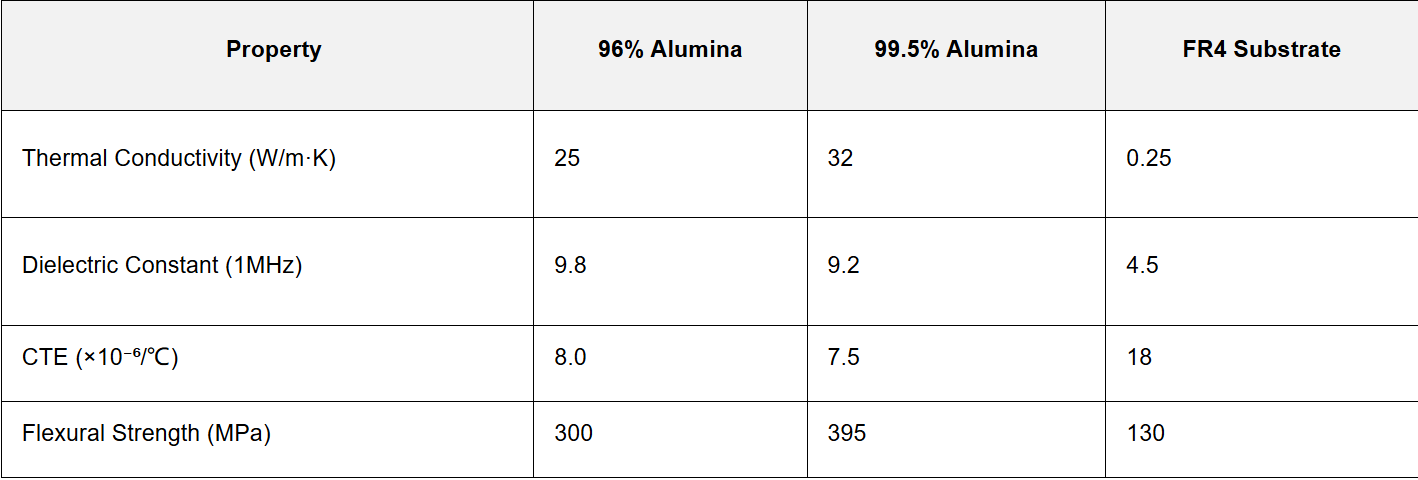
3. Design Implications of Material Properties
· Thermal Management: Using the thermal resistance model (θ=ΔT/P), heat dissipation paths can be quantified. For example, a 10mm×10mm×0.63mm 99.5% alumina substrate has a thermal resistance of just 0.31 K/W—90% lower than FR4.
· High-Frequency Performance: Low dielectric loss (tanδ<0.0002) reduces signal attenuation by 30% in 5G millimeter-wave bands (above 28 GHz).
Ⅲ. Manufacturing Processes and Quality Control
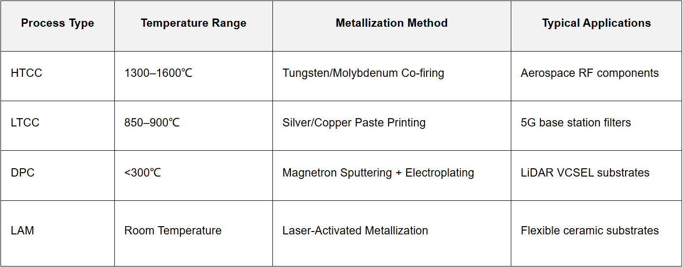
1. Comparison of Processes (Mainstream Processes)
2. Critical DPC Process Parameters
· Sputtering Thickness: Titanium/copper seed layers of 50–100 nm ensure adhesive strength >45 MPa.
· Electroplating Uniformity: Pulsed electroplating achieves copper thickness tolerance <±5% and linewidth precision ±10 μm.
· Laser Cutting: CO₂ laser processing ensures edge roughness Ra<1.6 μm to prevent micro-cracks.
3. Quality Inspection Standards
· IPC-6012 Class 3: Requires insulation resistance >10¹⁴ Ω·cm and no failure after 500 thermal cycles (-65℃ to 150℃).
· Thermal Shock Testing: Using a two-chamber thermal shock chamber with <10-second transition time and 30-minute dwell time, per GJB548B-2005.
Ⅳ. Engineering Design Guidelines
1. Thermal Management Design
· Thermal Resistance Optimization: Embedded copper pillars (0.3mm diameter, 1mm pitch) reduce thermal resistance by 40% while avoiding stress concentration.
· Heat Dissipation Path: Follow a three-stage architecture of "heat source → ceramic substrate → metal base," with interface thermal resistance <0.5 K/W.
2. Mechanical Stress Control
· Material Matching: For copper foil ≥0.3mm thickness, use a molybdenum-copper transition layer (CTE=6.5×10⁻⁶/℃) to reduce thermal stress cracking risk.
· Structural Design: 0.5mm-wide stress relief grooves at the substrate edge reduce warpage to <0.1%.
3. High-Frequency Circuit Design
· Impedance Control: 50Ω microstrip line width on 99.5% alumina substrate is calculated using:

· Parasitic Parameters: 3D electromagnetic simulation (e.g., HFSS) optimizes via structures to control parasitic inductance <0.5 nH.
Ⅴ. Typical Application Cases
1. New Energy Vehicle Electric Control Systems
· Tesla Model 3: 99.5% alumina DPC substrates in SiC power modules reduce thermal resistance to 0.14 K/W, supporting 800V high-voltage platforms.
· BYD Blade Battery BMS: 600mm×600mm large-format ceramic substrates integrate 16 independent acquisition channels, reducing wiring by 80%.
2. 5G Communication Base Stations
· Huawei AAU RF Units: HTCC-processed alumina substrates support 28 GHz signal transmission with power density up to 300 W/cm².
· ZTE Optical Modules: AlN/Al₂O₃ composite substrates in 100G PAM4 lasers boost thermal conductivity to 180 W/m·K.
3. Industrial Automation
· Siemens PLC Modules: LTCC-processed multilayer ceramic substrates integrate over 1,000 passive components, reducing volume by 50%.
· ABB Robot Controllers: LAM-processed flexible ceramic substrates enable operation in -40℃ to 150℃ wide temperature ranges.
Ⅵ. Industry Trends and Challenges
1. Technological Frontiers
· Thinning: Kyocera mass-produces 0.05mm-thick AlN substrates for chip-scale packaging (CSP).
· Function Integration: Embedded capacitor/resistor technology increases passive component density to 1,000 pF/mm².
· Green Manufacturing: Water-soluble etchant recycling systems achieve zero wastewater discharge, compliant with the EU New Battery Act.
2. Cost Optimization Strategies
· Material Substitution: 96% alumina substrates cost 60% of 99.5% variants, suitable for non-extreme thermal applications.
· Process Innovation: LAM technology reduces metallization costs by 30% while enabling rapid prototyping.
3. Testing Technology Breakthroughs
· T3ster Thermal Transient Testing: Measures junction temperature with 0.1℃ resolution—10x more precise than traditional infrared thermography.
· X-Ray Layer Scanning: Detects internal voids <5%, replacing destructive cross-section testing.
Ⅶ. Conclusion
Aluminum oxide ceramic-based PCBs have emerged as a core material for high-end electronics, driven by superior thermal management, high-frequency performance, and mechanical reliability. As processes like LAM and DPC mature, costs continue to decline, expanding application frontiers. With the rapid growth of 5G, new energy vehicles, and artificial intelligence, these PCBs will play an increasingly critical role in power electronics packaging.
Author: Jack Wang

