Unlocking PCB Manufacturing Capabilities for HDI, Rigid-Flex, and Flexible
PCBs (Printed Circuit Boards) are essential components in virtually all electronic devices, enabling the connection and functioning of various electronic components. From smartphones and computers to automotive systems and medical equipment, PCBs are critical for the performance and reliability of these products. As technology continues to advance, the demand for more efficient, compact, and reliable PCBs has grown, driving manufacturers to adopt more sophisticated production techniques.
For any company in the PCB manufacturing industry, strong PCB manufacturing capabilities are essential. These capabilities directly influence the quality, precision, and scalability of the PCBs produced, which in turn impacts the overall performance of the end products. A company’s ability to handle different types of PCBs—such as HDI, Rigid-Flex, and Flexible PCBs—requires expertise in specialized manufacturing processes and a commitment to maintaining high standards of quality control.
This article will focus on PCBMASTER’s capabilities in producing HDI, Rigid-Flex, and Flexible PCBs. We’ll explore how PCBMASTER addresses the unique challenges associated with each type of PCB, utilizing advanced manufacturing techniques to deliver high-quality, reliable solutions that meet the diverse needs of its clients.
PCBMASTER’s HDI PCB Manufacturing Capabilities
HDI PCB Definition and Applications
HDI PCBs are specialized circuit boards that allow for a higher density of components compared to traditional PCBs. These boards are characterized by smaller vias, tighter trace widths, and more complex multi-layer designs, enabling high-speed performance and more compact device designs. PCBMASTER uses cutting-edge manufacturing techniques to produce HDI PCBs that meet the rigorous standards of industries such as consumer electronics, telecommunications, and high-speed computing.
PCBMASTER’s HDI PCB Manufacturing Parameters
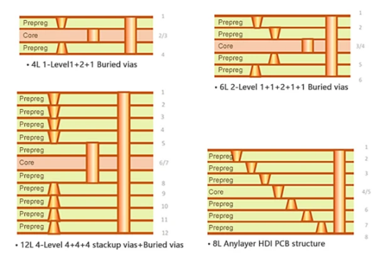
Layer Count and Stack-Up Design:
PCBMASTER offers flexibility in the number of layers for HDI PCBs. For mass production, it supports up to 24 layers, while for sample production, it can accommodate up to 60 layers. This flexibility allows PCBMASTER to cater to both simple and highly complex designs.
For the stack-up design, PCBMASTER provides multiple options:
3+N+3
4+N+4
AnyLayer (10L)
allowing for greater customization and more intricate designs.
Board Dimensions and Thickness:
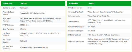
The maximum dimensions of the HDI PCBs that PCBMASTER can produce are 620mm × 1092mm. This expansion allows for larger designs without compromising the high-density requirements of modern electronics.
In terms of thickness, PCBMASTER supports a maximum board thickness of 3.2mm for standard designs and 4.2mm for more robust applications.
Impedance Tolerance:
Impedance control is critical for ensuring the signal integrity of high-speed PCBs. PCBMASTER guarantees tight impedance tolerances:
Differential Impedance (50 ohm): ±7%.
Single-Ended Impedance (50 ohm): ±6%.
Layer Registration and Alignment:
For accurate multi-layer stacking, PCBMASTER ensures precise layer alignment:
Up to 12 layers: Registration tolerance is ≥4 mil in 2025, improving to ≥3 mil in 2026.
More than 12 layers: Registration tolerance is ≥5 mil in 2025, improving to ≥4 mil by 2026.
Pattern Accuracy:
Precision in pattern accuracy is vital for the functionality of HDI PCBs, especially for small, tightly packed designs. PCBMASTER maintains:
±4 mil for boards up to 500mm in size.
±5 mil for boards exceeding 500mm in size, ensuring high-quality, consistent patterns across varying designs.
Special Capabilities
Laser Blind Hole:
To create high-density vias, PCBMASTER employs advanced laser drilling techniques. The capability ranges from 75/180um in 2025 to 65/165um by 2026, allowing for fine, precise drilling needed for miniaturized designs.
Plating and Dimple Control:
PCBMASTER ensures that the plating aspect ratio is high, supporting a 16:1, ensuring better via hole quality. The dimple size in plating is 10um, reflecting the precision in the manufacturing process.
Back-Drill Capabilities:
PCBMASTER’s back-drilling technology eliminates unwanted vias that could interfere with signal integrity. The minimum back-drill diameter is 0.4mm in 2025, improving to 0.35mm by 2026. The stub length is minimized from 6mil to 5mil, enhancing the overall electrical performance and ensuring lower signal loss.
Challenges and Solutions
Challenges:
The manufacturing of HDI PCBs presents several challenges, particularly due to the high precision required. The tight tolerances, intricate layer stacking, and complex via design necessitate advanced techniques and careful control throughout the production process. Additionally, maintaining high-speed performance and signal integrity across dense and compact designs is a significant challenge.
Solutions:
PCBMASTER addresses these challenges by continually innovating its manufacturing processes and adopting advanced technologies. Through strict quality control measures, automated testing systems, and the use of specialized processes like laser drilling and back-drilling, PCBMASTER ensures the highest levels of precision and performance. The company's commitment to ongoing research and development allows it to stay ahead of the curve, delivering reliable, high-quality HDI PCBs that meet the evolving demands of industries requiring miniaturized, high-performance electronics.
PCBMASTER’s Rigid-Flex PCB Manufacturing Capabilities
Rigid-Flex PCB Definition and Applications
Rigid-Flex PCBs combine the advantages of both rigid and flexible circuit boards, offering the reliability and support of rigid PCBs with the flexibility and adaptability of flexible PCBs. This combination allows for more complex and compact designs while maintaining durability and performance across a range of applications. PCBMASTER has developed advanced technologies in the production of Rigid-Flex PCBs, enabling it to meet the intricate demands of industries that require both flexibility and high performance in their electronic devices.
PCBMASTER’s Rigid-Flex PCB Manufacturing Parameters
Layer Count and Size:
PCBMASTER supports the production of Rigid-Flex PCBs with a range of layer counts, from simple designs to more complex configurations. PCBMASTER can produce Rigid-Flex PCBs with up to 30 layers for sample production. The maximum size of the PCB varies based on the design, with the company able to accommodate both small, compact designs and larger, more intricate assemblies.
Rigid and Flexible Areas:
One of the key challenges in Rigid-Flex PCB production is ensuring a seamless connection between the rigid and flexible parts of the board. PCBMASTER addresses this by using specialized techniques that ensure reliable bonding between these two materials, maintaining both electrical integrity and mechanical strength. The minimum copper-to-window distance is maintained at 0.2mm, while the minimum distance from the hole to the window is 0.4mm. These parameters ensure that the connection between rigid and flexible areas remains strong and stable over time, even under mechanical stress.
Special Processes:
PCBMASTER utilizes a variety of specialized techniques to enhance the manufacturing of Rigid-Flex PCBs:
Hybrid Lamination: This technology allows for a smooth transition between the rigid and flexible areas of the PCB, facilitating more complex designs and improving performance.
Plating: With copper thickness ranging from 0.33 oz to 2 oz for flexible areas and 0.33 oz to 4 oz for rigid areas, PCBMASTER ensures the optimal conductivity required for high-performance applications.
PTH Hole and Plating: The minimum completed PTH hole diameter is 0.1mm, enabling finer, more precise hole drilling for smaller designs.
Manufacturing Challenges and Solutions
Challenges:
The production of Rigid-Flex PCBs involves several unique challenges, particularly in the integration of rigid and flexible materials. One of the key difficulties is ensuring a seamless and durable connection between the rigid and flexible areas while maintaining the necessary mechanical strength and flexibility. Additionally, controlling the flatness of the board, as well as ensuring precise impedance control and pattern accuracy, can be challenging due to the multi-material nature of the design.
Solutions:
PCBMASTER has developed a series of strategies to address these challenges:
Improved Layer Control: Through the use of precise lamination and copper plating techniques, PCBMASTER ensures that both rigid and flexible areas meet high-quality standards for impedance control and durability.
Advanced Surface Treatment: The company uses specialized surface treatments to ensure that the flexible sections of the PCB maintain their flatness, with flatness tolerances of ≤0.50% to prevent warping or deformation during use.
Fine-Tuning of Critical Dimensions: PCBMASTER ensures that key dimensions, such as minimum line width/spacing (0.04mm) and hole size (0.1mm), are precisely controlled, allowing for complex designs with high component density and fine interconnections.
Special Technologies in Rigid-Flex PCB Manufacturing
RF Laser Stages:
For high-frequency applications, PCBMASTER offers RF laser stages with up to 3 stages, making it ideal for devices requiring low-loss, high-speed signal transmission. This technology is essential for products like 5G communication devices and high-speed computing systems that demand minimal signal interference.
Advanced Flex Circuit Capabilities:
PCBMASTER also provides flexible circuit options with specific requirements for RF (Radio Frequency) and hinged styles:
RF Flexible Circuits: The company supports up to 10 layers of flexible RF circuit designs for sample production and up to 8 layers for mass production, offering flexibility in handling complex RF designs.
Hinged and Bonded Flexible Circuits: PCBMASTER ensures that flexible circuits can be made with hinged or bonded configurations, which are ideal for applications that require bending or movement, such as wearable electronics.
PCBMASTER’s Flexible PCB Manufacturing Capabilities
Flexible PCB Definition and Applications
Flexible PCBs (FPCs) are specialized circuit boards that are built on flexible substrates, allowing them to bend, twist, and conform to various shapes without compromising electrical performance. PCBMASTER uses advanced technologies to produce flexible PCBs that meet the high-performance requirements of modern electronics. Unlike traditional rigid PCBs, FPCs offer enhanced durability, reduced space requirements, and increased design flexibility, making them ideal for applications that require compact, lightweight, and reliable circuits.
PCBMASTER’s Flexible PCB Manufacturing Parameters
Layer Count and Size:
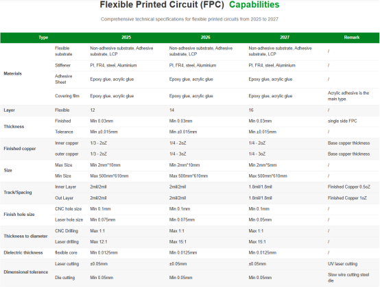
PCBMASTER supports flexible PCBs with up to 8 layers, making it suitable for complex designs with multiple interconnections. The manufacturing precision allows PCBMASTER to create flexible PCBs with the following size ranges:
Minimum Size: 5mm × 5mm, ideal for small, compact electronic devices.
Maximum Size: 500mm × 610mm, catering to larger, more intricate flexible PCB designs.
Manufacturing Precision and Thickness Control:
PCBMASTER ensures high precision in flexible PCB production:
Minimum Board Thickness: 0.03mm for single-sided flexible boards, allowing for ultra-thin designs.
Thickness Tolerance: ±0.015mm, ensuring uniformity in thickness and high-quality results for tight tolerance applications.
Finished Copper Thickness:
Inner Layer Copper: 1/3 oz to 2 oz.
Outer Layer Copper: 1/3 oz to 3 oz, providing the optimal balance between flexibility and conductivity for various applications.
Material Selection and Processing Techniques:
Flexible PCBs can be made using different base materials depending on the specific application:
Flexible Substrates: PCBMASTER uses both adhesive and non-adhesive base materials such as LCP (Liquid Crystal Polymer) and PI (Polyimide), known for their high temperature and chemical resistance.
Reinforcement Sheets: PI reinforcement, FR6 reinforcement, steel reinforcement, and aluminum reinforcement are used to provide additional strength where needed.
Bonding Sheets: Epoxy-based and acrylic-based adhesives are employed to bond layers of the flexible PCB, ensuring durability and high adhesion strength.
Special Processes:
To enhance the performance and manufacturability of flexible PCBs, PCBMASTER utilizes several specialized techniques:
Smooth Surface Treatment: To ensure high-quality, smooth surfaces, PCBMASTER employs advanced surface treatment techniques. This improves the reliability of component attachment and overall PCB performance.
Laser Cutting and Molding: PCBMASTER offers precise cutting with UV laser cutting capabilities, achieving ±0.05mm precision. Additionally, slow wire cutting is used for forming more intricate shapes and ensuring tight tolerances.
Challenges and Solutions in Flexible PCB Manufacturing
Challenges:
The production of flexible PCBs presents several challenges, particularly in terms of material selection, size limitations, and maintaining precision. Some key challenges include:
Material Variability: Different flexible substrates have varying thermal and mechanical properties, making it challenging to maintain uniformity and reliability across different production runs.
Size and Precision Limits: The thin and flexible nature of these PCBs makes it difficult to achieve precise hole sizes and controlled copper thickness without affecting the board’s performance.
Stress and Durability: Flexible PCBs are often subject to mechanical stress, which can lead to warping or damage. Ensuring the PCB can withstand bending and twisting without failure is a key challenge.
Solutions:
PCBMASTER addresses these challenges through continuous innovation and optimization:
Material Expertise: By selecting the right combination of flexible materials like PI and LCP, PCBMASTER ensures that the flexible PCBs meet both mechanical and electrical performance standards.
Advanced Manufacturing Processes: The use of high-precision laser drilling (down to 0.05mm hole sizes) and mechanical drilling (for larger hole sizes) allows PCBMASTER to meet tight specifications for hole diameters and feature sizes.
Enhanced Durability: To improve the mechanical strength of flexible PCBs, PCBMASTER incorporates reinforcement techniques such as PI reinforcement and steel reinforcement, ensuring the final product can handle stress, temperature fluctuations, and mechanical bending without compromising functionality.
Conclusion
PCBMASTER has built a strong reputation for its advanced manufacturing capabilities in HDI, Rigid-Flex, and Flexible PCBs. With state-of-the-art technologies, the company excels in producing high-density, reliable, and high-performance PCBs for industries such as telecommunications, automotive, and consumer electronics. Its expertise in layer stacking, precision drilling, impedance control, and specialized manufacturing processes positions PCBMASTER as a leader in PCB production.
As market demands evolve with the rise of 5G, AI, and IoT, PCBMASTER will continue to innovate, enhancing its manufacturing processes to support higher-performance and more complex designs. By embracing automation, AI, and sustainability initiatives, PCBMASTER is committed to staying ahead of industry trends, ensuring it meets the growing needs of the electronics market while maintaining quality, efficiency, and environmental responsibility.
FAQs
How does PCBMASTER ensure the high precision and reliability of HDI PCBs?
PCBMASTER ensures the high precision and reliability of HDI PCBs through advanced manufacturing techniques and strict quality control. The company employs precision drilling, laser via technology, and automated layer alignment to ensure high-density interconnects are produced with minimal defects. Additionally, PCBMASTER utilizes advanced impedance control and signal integrity management to maintain consistent performance in high-frequency applications. Regular electrical testing and automated optical inspection (AOI) are implemented to detect any potential issues early in the production process, guaranteeing a high level of reliability for the final product.
What are the special requirements for Rigid-Flex PCBs, and how does PCBMASTER meet them?
Rigid-Flex PCBs require a combination of rigid and flexible materials, which introduces specific challenges in ensuring a seamless connection between the two areas. PCBMASTER meets these demands through advanced lamination techniques, ensuring a smooth transition between the rigid and flexible sections without compromising performance. The company uses specialized materials such as PI (Polyimide) and LCP (Liquid Crystal Polymer) for flexibility and strength. Additionally, PCBMASTER ensures that the adhesion and mechanical strength between the rigid and flexible areas are robust, using reinforced laminates and precise alignment to ensure durability under bending, vibration, and temperature changes.
What are the special requirements for Flexible PCBs in medical devices, and how does PCBMASTER address them?
Flexible PCBs in medical devices must meet strict standards for biocompatibility, reliability, and durability. These devices often operate in environments that involve movement, temperature changes, and potential exposure to bodily fluids. PCBMASTER addresses these challenges by using biocompatible materials such as PI and LCP, which are resistant to chemicals and high temperatures. Additionally, the company employs rigorous reliability testing, including thermal cycling and mechanical stress tests, to ensure the long-term performance of flexible PCBs in medical applications. PCBMASTER also offers high-density designs for compact medical devices, ensuring that all circuits fit within small form factors while maintaining precision.
How does PCBMASTER address the challenges of high-speed signal transmission in PCB manufacturing?
The demand for high-speed signal transmission in modern electronics requires PCBs that can handle high frequencies with minimal signal loss or interference. PCBMASTER tackles this challenge by using advanced impedance control to ensure signal integrity and minimize reflection or attenuation. The company utilizes high-performance materials that reduce signal interference and ensure consistent electrical performance. Moreover, PCBMASTER implements precision manufacturing processes, such as laser drilling, microvia technology, and automated testing to ensure that high-speed signals are transmitted efficiently without degradation.
How will PCBMASTER enhance its PCB manufacturing capabilities to meet the more complex demands of the future market?
As the electronics industry continues to evolve, PCBMASTER will focus on innovation and technology integration to meet the more complex requirements of future designs. The company will invest in next-generation manufacturing technologies, including advanced automation, AI-driven quality control, and 3D PCB printing. These innovations will allow PCBMASTER to handle increasingly complex designs, such as multi-layer high-density interconnects (HDI), flexible and rigid-flex circuits, and miniaturized components. PCBMASTER will also continue to focus on sustainability, integrating eco-friendly materials and energy-efficient production methods to meet both market and environmental demands. Through these advancements, PCBMASTER aims to stay at the forefront of the PCB manufacturing industry, delivering high-performance solutions that meet the growing and evolving needs of the global market.