


Essential Guide to FPC Thickness Understanding Flexible Circuit Specs
Introduction
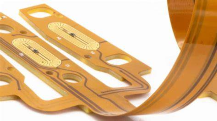
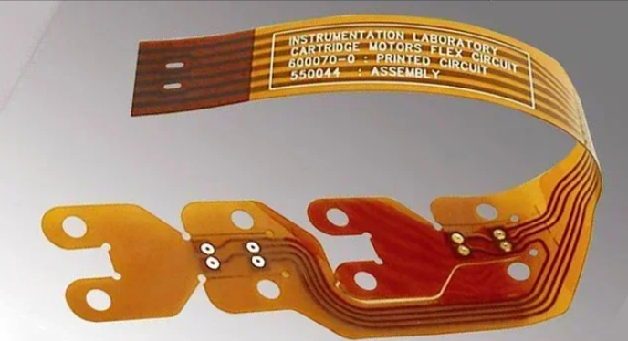
On a polyimide film thinner than a human hair, engineers weave intricate copper wire networks that serve as the lifeblood connecting modern electronic devices.
Every bend of a smartphone, every opening and closing of a foldable screen, every curve where a smartwatch conforms to the wrist—none of this would be possible without Flexible Printed Circuit (FPC) technology. Flex PCBs are constructed according to industry standards such as IPC-2223, with careful attention to design guidelines and material selection to ensure durability and performance. Flexible PCBs represent a broader category of circuit technology, and consulting with fabricators experienced in flexible circuits is essential to ensure design feasibility and reliability. The thickness design of an FPC is a delicate art of balancing performance, reliability, and cost in electronic devices.
As a key component in the miniaturization and flexibility of modern electronics, FPC thickness can range from a few micrometers to several hundred micrometers.
Why FPC Thickness Matters
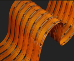
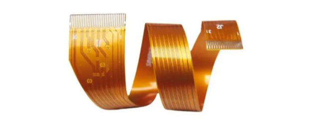
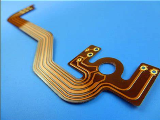
The thickness of an FPC directly impacts the design and performance of the entire electronic product. Unlike traditional rigid PCBs, these flexible circuits can bend, fold, and even stretch to fit complex spatial layouts.
The choice of thickness determines the board’s flexibility. The operating environment—such as exposure to high temperatures, mechanical stress, or repeated bending—plays a crucial role in selecting the appropriate FPC thickness and materials to ensure reliability and durability. Ultra-thin FPCs can bend like paper, while thicker ones offer better structural support. Thinner substrates and adhesive layers make the board more pliable, whereas thicker materials increase rigidity.
In FPC design, the thickness of the substrate and adhesive layers influences the board’s hardness and bending performance. The actual thickness of an FPC may differ from the design specification due to material properties and manufacturing tolerances. A thicker substrate generally offers higher mechanical strength. For instance, a 25μm thick substrate is a common and relatively cost-effective choice.
Flex Materials and Their Properties
The performance and reliability of any flex PCB start with the selection of its core materials. At the heart of every flexible circuit lies a polyimide film—renowned for its exceptional flexibility, mechanical strength, and ability to withstand high temperatures. Brands like Kapton have become industry standards, offering a stable base for intricate copper layers.
Copper foil forms the conductive pathways within the flex PCB. The choice of copper—whether rolled annealed for superior flexibility or electrodeposited for cost efficiency—directly impacts the board’s ability to endure repeated bending and maintain signal integrity. The copper layers’ thickness and quality also influence current-carrying capacity and overall board thickness.
Adhesives, often based on epoxy or acrylic chemistries, bond the copper foil to the polyimide substrate and can affect the flex PCB’s thickness, flexibility, and thermal performance. The adhesive’s properties must be carefully matched to the application’s requirements, especially in high-temperature or high-reliability environments.
A key property to consider is the dielectric constant of the polyimide film, which affects impedance control and signal transmission—critical for high-speed or controlled impedance designs. Similarly, the thermal performance of all flex materials determines how well the circuit board can operate in demanding environments, such as automotive or medical devices.
By understanding the unique properties of flex materials—dielectric constant, thermal performance, and mechanical strength—engineers can tailor their flex PCB designs for optimal performance, reliability, and longevity, even in the most challenging applications.
Bend Radius and Flex Life Considerations
When designing a flex PCB, the bend radius and flex life are two of the most important factors influencing long-term reliability. The bend radius is the minimum curve the flex board can safely achieve without risking cracks or delamination in the copper layers or substrate. A smaller bend radius allows for tighter folds and more compact device designs, but it also increases mechanical stress on the circuit.
Flex life refers to how many times a flex PCB can be bent before it shows signs of failure. Applications that require dynamic flexing—such as in foldable phones, wearable devices, or medical instruments—demand a high flex life to ensure the circuit remains functional over thousands or even millions of cycles.
Several factors affect both bend radius and flex life. Thinner boards, for example, can achieve a smaller bend radius and typically offer a longer flex life, as there is less material to resist the bending motion. The choice of flex materials, such as rolled annealed copper and high-quality polyimide, also plays a crucial role in enhancing durability and flexibility.
Designers can further optimize bend radius and flex life by carefully planning the layout—avoiding sharp corners, distributing traces evenly, and orienting copper traces perpendicular to the bend axis. Selecting the right thickness for each layer and using thinner boards in the flex area can significantly improve performance in dynamic applications.
By prioritizing bend radius and flex life during the design phase, engineers can ensure their flex PCBs deliver reliable performance, even in the most demanding environments where repeated bending is the norm.
Key Considerations in FPC and Copper Thickness Design and Selection
Designing and selecting FPC thickness requires a holistic approach, considering multiple factors. The primary consideration is the application scenario—will the board undergo frequent flexing, or will it remain static after installation?
For applications involving repeated bending, it is advisable to opt for thinner substrates and adhesive layers. This reduces stress on the copper foil surface, thereby minimizing the risk of micro-cracks. Single-layer designs are often best suited for such uses. Single layer boards are the thinnest and most flexible type of FPC, making them ideal for compact or highly flexible electronic applications.
Common substrate thicknesses include 12.5μm, 25μm, and 50μm, with 25μm and 50μm polyimide substrates being the most prevalent.
Copper foil thickness typically comes in four variants: 1/3 OZ (approx. 12μm), 1/2 OZ (approx. 18μm), 1 OZ (approx. 35μm), and 2 OZ (approx. 70μm). Thinner copper foils facilitate finer line widths and spacing.
Stiffeners also affect the overall thickness. Common stiffening materials include PI, PET, FR4, and metal plates, usually starting at 125μm or customized as needed.
When considering double-sided or multilayer boards, the layer count—how many layers are included—directly impacts the total FPC thickness. Adding more layers results in a thicker, less flexible board. Multilayer flex designs require careful stack up planning to maintain flexibility and durability, as the arrangement of flex layers within the stack up can optimize both performance and mechanical strength.
Table: Common FPC Material Thickness Specifications
| Material Type | Common Thickness Specifications | Primary Applications |
|---|---|---|
| Substrate | 12.5μm, 25μm, 50μm, 75μm, 125μm | Main board structure |
| Copper Foil | 12μm (1/3OZ), 18μm (1/2OZ), 35μm (1OZ), 70μm (2OZ) | Conductive traces |
| Coverlay | 12.5μm, 25μm | Circuit protection |
| Stiffener | 125μm and above, customizable | Local support and reinforcement |
Adhesive thickness must be carefully selected to ensure proper bonding and maintain flexibility. Adhesive based materials, while common, can introduce manufacturing challenges such as moisture absorption, dimensional errors, and potential issues like adhesive squeeze-out and via cracks.
Cost Comparison of FPCs with Different Thicknesses
The cost structure of FPCs is complex, with thickness being a significant factor. Material costs generally increase linearly with thickness, but the complexity of the manufacturing process can have a non-linear impact on the final price. Copper weight, typically measured in ounces per square foot, directly impacts both material cost and the current-carrying capacity of the board.
Ultra-thin FPCs often require more expensive materials and more precise fabrication techniques. For example, FPCs using adhesiveless substrates (a two-layer structure of just copper foil and substrate) are more costly and are typically used in products requiring over 100,000 flex cycles.
Rolled copper is more expensive than electrodeposited copper but offers superior mechanical properties and flex endurance, making it the preferred choice for products with high bending requirements. Copper plating and button plating processes are used to control copper thickness and ensure reliable electrical performance, which can also affect manufacturing costs.
The type and thickness of the adhesive layer also influence cost. Epoxy and acrylic adhesives are the most common, with epoxy being more widely used. Adhesive layer thickness typically ranges from 0.4 to 2 mils (approx. 10 to 50μm), with 0.72 mils (approx. 18μm) being a standard choice.
From a structural perspective, double-sided and multilayer boards are significantly more expensive than single-sided ones due to the increased material usage and more complex manufacturing processes. Multilayer FPCs are particularly costly to produce, as they require drilling and plating to create vias that form conductive paths between layers. Thicker copper and thicker boards increase both material and processing costs, and wider traces may be required for high-power applications, further impacting cost.
Pros and Cons of Thin, Medium, and Thick FPCs
FPCs can be categorized into thin (total thickness < 0.1mm), medium (total thickness 0.1-0.3mm), and thick (total thickness > 0.3mm) types, each with distinct advantages and disadvantages. Most flex PCBs fall within the 0.1-0.3mm range, as defined by industry standards such as IPC-6013 and IPC-2223, balancing flexibility and durability for common applications.
Ultra-thin FPCs (typically < 0.1mm) offer exceptional flexibility, making them ideal for space-constrained applications requiring frequent bending, such as the hinge area in foldable phones. However, their mechanical strength is lower, making them more susceptible to damage. Installation and soldering are more challenging, and the demanding manufacturing process leads to significantly higher costs.
Medium-thickness FPCs (0.1-0.3mm) strike a good balance between flexibility and strength, making them the most common type in consumer electronics. They provide sufficient mechanical support for component mounting while retaining a moderate bending capability. However, they are not suitable for extreme bending applications and may lack the robustness required for high-reliability industrial environments.
Thick FPCs (> 0.3mm) offer excellent mechanical strength and heat dissipation, suiting applications with heavier components or greater thermal demands, such as automotive electronics and industrial control systems. The selection and testing of raw materials, guided by standards like IPC-6013, play a crucial role in determining the thickness and properties of the final board. Their main drawbacks are limited flexibility, resistance to bending, increased weight, and unsuitability for space-constrained designs.
Best Practices for FPC Thickness Design
When designing FPC thickness, engineers should follow established best practices and design rules in pcb design for flexible and rigid flex circuits to ensure the final product’s performance and reliability.
First, clearly define the bending requirements. For applications involving repeated flexing, rolled copper foil should be used, ensuring the foil’s grain direction aligns with the primary bending axis of the board. Circuit traces should run perpendicular to the bend direction and be evenly distributed across the flex section and bend area to manage strain and improve durability.
During routing, trace width and spacing should be optimized based on copper foil thickness. Thinner foil allows for smaller line width and spacing but reduces current-carrying capacity. In typical FPC designs, the minimum line width/space can reach 35μm/50μm. For high speed signals, controlled impedance is critical, and surface finishes are used to protect copper traces and ensure solderability.
For the FPC outline, the minimum internal bend radius should be 1.5mm or greater. A larger radius enhances reliability and tear resistance. Any slit or slot in the flexible area must terminate in a circular hole with a diameter of at least 1.5mm to prevent tearing. Managing the bend area, setting a static bend, and using stiffeners in the flex section are important for maintaining mechanical support and durability.
In multilayer FPCs, areas subject to frequent bending during use should incorporate air gap layers and use thinner PI materials to increase pliability. Polyimide layers are commonly used as dielectric insulators and coverlay materials. The stackup often integrates flex sections and flexible regions to accommodate mechanical flexibility and prevent circuit breakage during repeated flexing.
When creating openings in the coverlay, ensure the pad size is larger than the coverlay opening. This prevents adhesive squeeze-out from reducing the pad size and creating irregular edges. In such cases, using a thinner adhesive (e.g., 13μm) is advisable. Rigid flex pcb design and rigid flex design require careful planning of rigid and flexible regions, including rigid sections and rigid flex boards, to ensure mechanical support and reliability.
Flex circuits and flexible regions play a key role in advanced electronic assemblies, while rigid flex pcbs combine rigid and flexible regions for optimal performance, reliability, and structural stability in complex applications.
Conclusion
The FPC connecting the mainboard to the screen in a smartphone can be as thin as 0.1mm—about two-thirds the thickness of a standard sheet of printer paper. Yet, this delicate circuit board can withstand hundreds of bends daily. By precisely calculating the copper foil's grain direction and substrate thickness, engineers can extend its service life to an impressive 100,000+ flex cycles.
The moment a foldable phone screen unfurls, meticulously arranged FPC traces are quietly transmitting electrical signals. On the curved surface where a smartwatch meets the wrist, ultra-thin FPCs conform to the case's contour, delivering commands from the chip to every pixel on the display.
Selecting FPC thickness is an integrated art combining materials science, mechanical engineering, and cost control. It directly shapes the form and future of electronic products.
FAQs
Q: What is the common thickness range for FPCs?
A: The typical overall thickness ranges from 0.05 mm to 1.5 mm. Ultra-thin variants can be as slim as 0.05 mm, while common thicknesses of 0.1–0.3 mm are suitable for consumer electronics such as smartphones. Thicknesses of 0.4–0.5 mm are better suited for applications requiring higher mechanical strength.
Q: What layers contribute to FPC thickness?
A: Thickness results from the cumulative layers of materials. Core components include the PI substrate, copper foil, coverlay, and—for adhesive-based constructions—the adhesive layer. Additional layers such as shielding or stiffeners must also be factored in for corresponding product types.
Q: Why does the measured FPC thickness often differ from the ordered specification?
A: Variations arise from structural differences across regions. For example, areas with openings lack coverlay, and soldering finger zones may have no coverlay on either side. Measurements taken in these regions will naturally reflect a reduced thickness.
Q: Does copper thickness significantly affect overall FPC thickness?
A: Yes, it has a notable impact. Common copper weights include 0.5 oz (~0.017 mm), 1 oz (~0.034 mm), and 2 oz (~0.068 mm). Thicker copper increases total thickness and may also require a thicker adhesive layer—1 oz copper foil typically pairs with a heavier adhesive.
Q: Does white coverlay affect FPC thickness?
A: Yes. White coverlay includes an additional white coating compared to standard yellow coverlay. This adds approximately 18 µm to the thickness for single-sided boards and about 36 µm for double-sided boards.
Q: Is stiffener thickness included in the nominal FPC thickness?
A: Typically not. The nominal FPC thickness generally refers only to the flexible circuit itself. The total thickness in stiffened areas requires adding the stiffener material's thickness, factoring in solder mask and copper layering during calculation.
Q: How does thickness relate to FPC bending performance?
A: Thinner boards generally offer better bend performance. For instance, the minimum bend radius for single-layer boards is 3–6 times the conductor thickness, while multilayer boards require 10–15 times. Dynamic bending applications particularly demand thinner constructions.
Author: Jack Wang

