


Understanding 01005 0402 Chip Size Parts: Essential Guidelines for PCB Design
The 01005 0402 chip size parts are essential for modern electronics due to their small size and efficiency. This article explains their dimensions, uses, and how to design PCBs with these components.
Key Takeaways
·01005 and 0402 chip size parts are critical for modern electronics, with their small dimensions enabling more efficient use of space in devices.
·Accurate land patterns and footprints are essential for reliable PCB designs, requiring adherence to standards to mitigate issues like solder bridging.
·Utilizing 01005 and 0402 components involves higher assembly costs due to the need for specialized equipment and techniques, underscoring the importance of meticulous design and cost management.
What Are 01005 and 0402 Chip Size Parts?
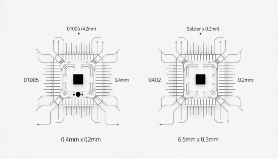
Understanding the dimensions and applications of 01005 and 0402 chip size parts highlights their significance. The 01005 chip size measures a mere 0.4 mm by 0.2 mm, which translates to approximately 0.016 inches by 0.008 inches—an impressive feat of miniaturization. The 0402 chip size, slightly larger, measures 1.0 mm by 0.5 mm, or about 0.040 inches by 0.020 inches. Despite their tiny footprints, these components are integral to various advanced electronic devices, showcasing their actual physical size.
These components are integral to numerous high-tech applications. They are commonly used in mobile devices, wearables, and other compact electronic products where space is a premium. The push for smaller, more efficient circuit boards has made these chip sizes a favorite among designers and engineers alike.
The ability to shrink components without sacrificing performance is invaluable in a world where the number of features packed into a single device keeps growing. As technology advances, the demand for smaller chip sizes will grow, requiring designers to stay current with these trends and associated design service considerations to maintain a clear view of the multiple models area market, making a distinction in their result offerings.
Whether you’re referring to datasheets or working on a new circuit board design, to learn about these components is the first step toward creating cutting-edge electronics.
Land Patterns for 01005 and 0402 Components
Accurate land pattern patterns are the backbone of reliable PCB designs, especially when working with a lot of 01005 and 0402 components. Precisely defining land patterns is crucial for both performance and assembly. Proper footprint design is vital, as even minor errors can cause significant issues like solder bridging or cold joints.
·When designing footprints for 0402 components, consider the following:
·Ensure adequate clearance between pads to prevent solder bridging during the soldering process.
·Align pads with component terminals to minimize soldering errors.
·Adhere to standards such as IPC-7351 to accurately define these patterns, facilitating smoother assembly and reducing the risk of defects.
Following these guidelines enables designers to create reliable and efficient PCB layouts. The arrangement of land patterns must consider the component’s pcb footprint, ensuring that areas around the pads are sufficient to avoid any bridging or misalignment. Accurate land patterns designed improve both the manufacturability and overall reliability and performance of the board.
Challenges in Soldering 01005 and 0402 Parts

Soldering 01005 and 0402 parts requires specialized machinery and precision techniques due to their unique challenges. These components’ small dimensions make manual soldering impractical, necessitating the use of advanced equipment. This need for specialized machinery often leads to higher assembly costs, a factor that cannot be ignored. The processes require parts to be soldered with care to ensure reliability.
Applying solder paste to these tiny components is one of the most significant challenges. For 01005 parts, stencil apertures must be extremely small, requiring precise technology for consistent deposits. Minor misalignments of 50-100 µm during placement can cause short circuits or unreliable connections, emphasizing the need for accuracy.
Thermal management is another crucial consideration. Reflow soldering requires careful temperature control to avoid damaging these components. The risk of overheating during manual rework is high, as standard tools may not provide the precision needed for such tiny sizes. Adhering to IPC standards mitigates many soldering defects, ensuring a more reliable assembly process.
Maintaining strict component placement accuracy is crucial. Slight misalignments can lead to catastrophic defects, highlighting the importance of precision in soldering. Meticulously following all assembly processes helps avoid common issues and results in a reliable circuit board.
Best Practices for Designing with 01005 and 0402 Parts
A meticulous approach is required when designing with 01005 and 0402 parts to ensure reliability and performance. Adequate clearance around these components prevents unintentional short circuits and is crucial for proper soldering.
Designing traces to minimize their length reduces inductance, important in high-frequency applications. Using a pad size that exceeds the component’s footprint enhances solder joint reliability by accommodating potential misalignments during assembly.
Incorporating teardrops enhances the electrical connection between traces and pads, especially for smaller chip sizes. High-quality stencils are crucial for precise solder paste application, particularly for 01005 components.
While 01005 components are ideal for high-density applications, 0402 components offer a balance between size and ease of handling in circuit designs. Following these best practices enables designers to create robust and efficient PCBs.
Component Footprints and Libraries
Comprehensive component libraries are a game-changer for PCB designers. With over 10 million parts available, designers can quickly find and integrate the necessary component footprints into their designs. Tools like Altium, Eagle, and KiCad streamline the design process by allowing direct download of these footprints.
Real-time automated check determines the manufacturability of a footprint, preventing costly design errors. Custom footprints can be efficiently created for parts not yet in libraries using computer-vision tools and library requests.
Access to vast libraries and tools allows designers to build accurate and reliable PCBs for free. It facilitates seamless integration of components into designs, reducing the time and effort required for manual footprint creation. Access to extensive resources ultimately enhances the efficiency and accuracy of the design process.
Ensuring Reliability with 01005 and 0402 Components
The reliability of solder joints for 01005 and 0402 components is paramount. Choosing between solder mask defined and non-solder mask defined pads greatly influences the reliability of solder joints.
Meticulously checking and ensuring pad definitions significantly enhances PCB reliability. Accuracy in these details ensures components maintain their integrity and performance over time.
Cost Considerations for Using Small Chip Size Parts
Using 01005 and 0402 chip size parts can significantly impact overall PCB fabrication and assembly costs. The precision equipment and techniques needed for these smaller components often lead to higher fabrication costs. Assembly costs may rise due to the increased complexity and specialized processes needed for proper placement and soldering.
When budgeting for PCB production, account for both fabrication and assembly costs related to 01005 and 0402 parts to avoid unexpected expenses. Despite higher costs, the advantages of using smaller components—like more efficient use of space and enhanced performance—often outweigh the financial considerations.
Understanding these cost implications allows designers to balance the benefits of miniaturization with associated expenses. Effective planning and budgeting can lead to the creation of advanced and efficient PCBs using small chip size parts.
Industry Standards and IPC Guidelines
Adhering to industry standards and IPC guidelines ensures the quality and reliability of electronic products. IPC standards offer comprehensive guidelines on PCB design and assembly processes, ensuring adherence to best practices.
Following IPC-2221 standards ensures proper design practices for PCB layouts that include components as small as 01005. Standards for pad size and clearance significantly improve manufacturability and reduce defects during PCB production. IPC-A-610 outlines the acceptability of electronic assemblies, crucial for components like 01005 and 0402.
Staying up to date with these standards allows designers to create better products, enhance reliability, and reduce defects. Adhering to IPC guidelines is a vital step in producing high-quality electronic assemblies.
Summary
In conclusion, the integration of 01005 and 0402 chip size parts into PCB designs requires careful consideration and adherence to best practices. From understanding their dimensions and applications to mastering land patterns, soldering challenges, and industry standards, each step is crucial for creating reliable and high-performance PCBs.
By focusing on precision, reliability, and adherence to standards, designers can overcome the challenges associated with these tiny components. The journey of miniaturization is filled with technical details, but the rewards in terms of advanced, compact, and efficient electronic products are well worth the effort.
Frequently Asked Questions
What are the dimensions of 01005 chip size parts?
The dimensions of 01005 chip size parts are 0.4 mm by 0.2 mm, which is approximately 0.016 inches by 0.008 inches.
What are some common applications for 01005 and 0402 chip size parts?
Common applications for 01005 and 0402 chip size parts include mobile devices, wearables, and other compact electronic products, reflecting the industry's need for small, efficient components.
Why are accurate land patterns important for 01005 and 0402 components?
Accurate land patterns are crucial for 01005 and 0402 components as they ensure reliable performance and facilitate proper assembly, thereby preventing potential solder bridging and misalignment issues.
What challenges are associated with soldering 01005 components?
Soldering 01005 components presents significant challenges primarily due to their diminutive size, which necessitates specialized machinery, precise application of solder paste, and meticulous thermal management. These factors contribute to an increased complexity in the soldering process.
How do IPC standards help in designing with 01005 and 0402 parts?
IPC standards enhance the design of 01005 and 0402 parts by offering specific guidelines on pad size and clearance, which ultimately improves manufacturability and minimizes defects in PCB production.

