


Top Tips for Perfect PCB Assembly Drawings Every Engineer Should Know
Creating a flawless PCB assembly drawing is more than just a technical task—it’s the bridge between your design and a perfectly functioning product. Even the smallest mistake in component placement or labeling can lead to costly rework and production delays. In this guide, we’ll walk you through top tips every engineer should know to craft accurate, clear, and error-free PCB assembly drawings. Whether you’re a beginner or a seasoned designer, these insights will help you streamline your workflow, avoid common pitfalls, and ensure your designs translate seamlessly from screen to assembly line.
Introduction to PCB Assembly Drawings
What is a PCB Assembly Drawing?
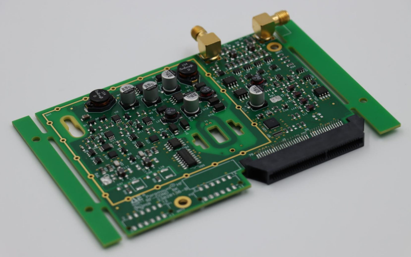
A PCB assembly drawing is a detailed diagram that shows the exact placement, orientation, and identification of all components on a printed circuit board (PCB). Its primary purpose is to guide the assembly process, ensuring that every part is correctly installed during manufacturing. Unlike a PCB layout, which focuses on the routing of traces and electrical connections, or a schematic, which shows the circuit’s functional design, the assembly drawing is specifically designed for production use.
Example: While a schematic might indicate a resistor connects between two points, the assembly drawing shows the resistor’s exact location, rotation, and reference designator on the board. This distinction helps manufacturers translate designs from paper or software into a real, functional PCB.
Importance of Accurate PCB Assembly Drawings
Accurate assembly drawings are essential for smooth PCB production. They offer several tangible benefits:
Reduces manufacturing errors: Clear component placement, orientation, and labeling help prevent mistakes like reversed polarity or misplaced parts.
Saves time and cost during assembly: Precise drawings reduce trial-and-error on the assembly line, minimizing rework and wasted components.
Improves communication between designers, manufacturers, and assemblers: Standardized drawings ensure that everyone involved in production understands the design intent, reducing misinterpretations and delays.
Comparison: Consider two PCB assembly drawings for the same board: one detailed and standardized, the other vague and inconsistent. The detailed drawing results in a smooth assembly process, while the vague drawing often leads to errors, delays, and extra costs.
Common Challenges in PCB Assembly Drawings
Even experienced engineers can encounter issues when creating assembly drawings. Some frequent challenges include:
Misplaced components or unclear labeling: Components without proper reference designators or ambiguous placement can confuse assemblers.
Missing mechanical or reference details: Omitting mounting holes, keep-out zones, or board outlines can result in improper component fitting.
Inconsistent design conventions: Using different symbols, annotations, or measurement units across a drawing can lead to errors during manufacturing.
Step-by-Step Tip: To avoid these problems, always cross-check component placement against the schematic, verify mechanical details, and apply standardized symbols consistently.
Essential Elements of a PCB Assembly Drawing
Component Placement and Orientation
Proper component placement and orientation is crucial to ensure the PCB functions correctly and can be efficiently assembled.
Step-by-Step Guidelines:
1. Mark Top and Bottom Sides: Clearly indicate which components go on the top layer and which on the bottom.
2. Check Polarity: Highlight polarized components like diodes, LEDs, and electrolytic capacitors. Use standard polarity markings (+/-) to prevent reverse installation.
3. Indicate Rotation: Show the correct rotation for components like ICs, connectors, and polarized capacitors. Include pin 1 indicators for ICs.
Example: A reversed LED or electrolytic capacitor can cause circuit failure. In contrast, a clearly marked assembly drawing ensures the component is installed correctly the first time.
Bill of Materials (BOM) Integration
Integrating the BOM with the assembly drawing streamlines manufacturing and reduces errors.
Best Practices:
Link Components to BOM Efficiently: Reference each component by its designator (e.g., R1, C2) and link it to the BOM.
Ensure Accuracy: Include correct part numbers, values, and specifications. Double-check that every component in the BOM is represented on the drawing.
Comparison:
Manual BOM Updates: Time-consuming and prone to mistakes.
Automated BOM Integration: Updates component data automatically, reducing errors and improving efficiency.
Mechanical and Reference Details
Mechanical information ensures the board fits correctly in its enclosure and avoids conflicts during assembly.
Key Elements to Include:
Mounting holes and their diameters.
Keep-out areas for connectors, heat sinks, or other components.
Board outlines and dimensions.
Step-by-Step Annotation:
1. Draw the board outline with precise dimensions.
2. Mark all mounting holes with correct diameters and positions.
3. Identify any areas that should remain free of components.
Example: A missing keep-out area can result in a tall capacitor colliding with the case, requiring costly rework.
Layer and Silkscreen Considerations
Clear silkscreen and layer markings are essential for efficient assembly and inspection.
Tips:
Silkscreen Clarity: Use readable fonts and consistent sizes. Avoid overlapping text or symbols.
Top vs. Bottom Layers: Differentiate clearly between components on top and bottom layers using labels or colors.
Best Practices Example:
Mark all reference designators on the top layer with a clear font and orientation that matches the component placement.
Use outlines to show component pads, making assembly verification faster.
Design Conventions and Standards
Industry Standards to Follow
Following industry standards ensures that PCB assembly drawings are clear, consistent, and compatible with manufacturing processes.
IPC-2612: Defines the standard format and content for PCB assembly drawings. It covers component placement, reference designators, and layer information.
IPC-2581B: A standardized, machine-readable format for exchanging PCB design, fabrication, and assembly data, enhancing automation, reducing errors, and supporting complex board types such as HDI and rigid-flex PCBs.
Benefits:
Reduces errors by ensuring all manufacturers interpret drawings consistently.
Improves compatibility between different software tools and assembly facilities.
Facilitates automation and data exchange across teams.
Example: A PCB assembly drawing following IPC-2612 clearly shows pin 1 orientation, component designators, and layer information, making it easier for any assembler to work without confusion.
Consistent Symbols and Annotations
Using consistent symbols and annotations avoids misinterpretation and ensures accurate assembly.
Step-by-Step Guide:
1. Choose a standardized set of symbols for resistors, capacitors, diodes, ICs, and connectors.
2. Use the same font and size for all reference designators.
3. Annotate special requirements like polarity, orientation, or mechanical constraints clearly.
Comparison:
Confused Symbols: Using multiple symbols for the same component (e.g., different diode symbols) can cause assembly errors.
Standardized Symbols: Using consistent, recognized symbols ensures every assembler interprets the drawing correctly.
Example: Marking all polarized capacitors with a plus (+) sign and consistent orientation arrows reduces the risk of reverse installation.
Clear Dimensioning and Tolerances
Accurate dimensioning and tolerances help ensure components fit precisely and function reliably.
Specifying Placement Tolerances
Clearly indicate acceptable placement deviations for each component. Include tolerances for X, Y positions and rotation angles when needed.
Step-by-Step Tips:
1. Mark reference points or datums on the PCB.
2. Specify the maximum allowable deviation from the ideal placement.
3. Use clear units (mm or mils) and consistent symbols for tolerances.
Example:
Effective Annotation: R1 ±0.1 mm, Pin 1 orientation marked with arrow.
Confusing Annotation: Only showing R1 location without tolerance or orientation, leading to assembly errors.
Benefit: Proper dimensioning ensures all components are installed correctly, reduces rework, and improves overall product quality.
Tips for Optimizing PCB Assembly Drawings
Use Layer Colors and Markings Wisely
Using layer colors and markings effectively improves readability and reduces assembly errors.
Recommended Color Codes:
Top layer: green
Bottom layer: blue
Silkscreen: white or yellow
Critical nets or signals: red or orange
Examples: Highlight high-current traces, power nets, or critical components using bright or contrasting colors. This makes them stand out for assemblers and inspectors.
Benefit: Proper color usage quickly communicates important information, reducing misinterpretation during assembly.
Simplify and Avoid Clutter
A clean assembly drawing is easier to read and less prone to errors.
Step-by-Step Methods:
1. Group related components together logically.
2. Remove unnecessary lines, labels, or overlapping annotations.
3. Use callouts or separate detail views for dense areas.
Comparison:
Clean Drawing: Components are clearly placed, labels are legible, and critical areas are highlighted.
Overloaded Drawing: Overlapping text, crowded symbols, and confusing annotations increase the likelihood of assembly mistakes.
Example: Separating densely packed IC pins into a zoomed detail view prevents misreading pin assignments.
Check for Common Errors
Performing a pre-production check ensures the assembly drawing is accurate.
Checklist:
Correct component orientation and polarity.
Presence of all reference designators.
Alignment of components with mechanical constraints.
Completeness of layer and silkscreen information.
Example of QA Process:
1. Cross-check all components against the BOM.
2. Verify pin 1 orientation for all ICs.
3. Confirm mounting holes and keep-out zones match mechanical requirements.
4. Document and fix any discrepancies before sending drawings to production.
Collaboration with Manufacturers
Effective collaboration with manufacturers reduces errors and improves assembly efficiency.
Best Practices:
Share drawings in standardized formats (e.g., IPC-2581, Gerber).
Include clear notes for special requirements.
Maintain open feedback loops to address questions or suggestions.
Step-by-Step Integration of Manufacturer Notes:
1. Send initial drawings to the manufacturer.
2. Review manufacturer comments and clarify ambiguities.
3. Update drawings to incorporate feedback.
4. Confirm final approval before production starts.
Benefit: Early collaboration helps prevent costly rework, ensures manufacturability, and improves overall product quality.
Tools and Software for PCB Assembly Drawings
Popular PCB CAD Tools
Several PCB CAD tools are widely used to create assembly drawings. Each has unique strengths and limitations:
Strengths: User-friendly, widely supported, good for small to medium projects.
Limitations: Limited advanced features for large, complex boards.
Strengths: Comprehensive feature set, advanced 3D visualization, integrated BOM management.
Limitations: Higher cost, steeper learning curve for beginners.
Strengths: Open-source, flexible, growing community support.
Limitations: Less automation compared to premium tools; some advanced features require manual setup.
Example: An engineer using Altium can link components directly to the BOM and generate accurate assembly drawings with minimal manual annotation, saving time and reducing errors.
Automated vs Manual Drawing Techniques
Automation in PCB assembly drawings helps reduce human errors and streamline production.
Manual Annotation:
Pros: Complete control over every detail.
Cons: Time-consuming, prone to mistakes such as mislabeling or missing components.
Automated Drawing Techniques:
Pros: Automatically links components to the BOM, applies standardized symbols, and updates changes in real time.
Cons: May require learning software-specific workflows.
Comparison Example:
Manual: Updating 200 components by hand can result in missed reference designators.
Automated: Software updates all 200 components instantly when the BOM changes, reducing risk of errors.
Using AI or DRC Checks
Design Rule Check (DRC) tools and AI-assisted verification enhance the accuracy of assembly drawings.
Benefits:
Detects misplaced components, incorrect clearances, and layer inconsistencies.
Ensures compliance with manufacturing standards before production.
Step-by-Step: Using DRC or AI Checks:
1. Load the assembly drawing in the PCB CAD tool.
2. Run the DRC to check for spacing, placement, and polarity errors.
3. Review flagged issues and make corrections.
4. Optionally, use AI-assisted suggestions to optimize component placement and annotations.
5. Save and recheck to ensure all issues are resolved.
Example: A DRC might flag a capacitor placed too close to a mounting hole, preventing a potential assembly failure. AI tools can suggest repositioning automatically.

Real-World Examples and Case Studies
Example of a Well-Executed PCB Assembly Drawing
A well-executed PCB assembly drawing combines clear layout, accurate annotations, and complete BOM integration to ensure smooth production.
Step-by-Step Reasoning:
1. Layout Planning: Components are arranged logically, grouping related parts close together to minimize trace lengths and assembly complexity.
2. Annotations: All reference designators, polarity markers, and rotation indicators are clearly labeled. Critical components, such as power regulators and connectors, are highlighted.
3. BOM Integration: Each component is linked to the BOM with part numbers, values, and specifications, ensuring the manufacturer can source the correct parts without confusion.
4. Verification: DRC checks and visual reviews confirm component placement, silkscreen clarity, and mechanical fit.
Example Outcome: The drawing enables the assembly team to install all components correctly on the first try, reducing rework and production delays.
Lessons Learned from Common Mistakes
Even small errors in assembly drawings can lead to costly rework and production delays.
Case Study:
During a production run, a PCB was sent for assembly with several issues. The integrated circuits (ICs) were installed in the wrong orientation, and the polarized capacitors were reversed. In addition, some connectors were misaligned, causing interference with the enclosure.
As a result, rework was required, delaying the project by several days and increasing costs.
Comparison:
Pre-Checked Drawing: By verifying component orientation, reference designators, and mechanical constraints beforehand, production proceeded smoothly with zero rework.
Post-Production Issues: Lack of pre-checks resulted in assembly errors, wasted components, and additional labor.
Key Takeaway: Conducting thorough reviews, including DRC checks, BOM verification, and mechanical alignment validation, prevents common mistakes and ensures reliable PCB assembly.
Conclusion
Creating accurate PCB assembly drawings requires careful attention to component placement, orientation, BOM integration, mechanical details, and layer markings, all while following industry standards. Clear design conventions, effective use of CAD tools, and thorough pre-production checks are essential for reliable and efficient assembly.
Applying these best practices reduces errors, speeds up production, and improves cost-effectiveness. For example, verifying component orientation and integrating the BOM correctly can prevent costly rework and ensure a smooth transition from design to manufacturing.
PCB assembly drawings should also be continuously refined based on lessons learned from past projects. Regular updates, reviewing errors, and incorporating manufacturer feedback help achieve higher-quality outcomes.
If you have further questions or want to learn more about PCBs, PCBMASTER, a professional PCB supplier, is ready to provide expert guidance and answer any inquiries.
FAQs
What is the difference between a PCB assembly drawing and a schematic?
A PCB schematic is a diagram that represents the functional connections of a circuit. It shows how components like resistors, capacitors, and ICs are electrically connected but does not indicate their physical placement on a board. In contrast, a PCB assembly drawing provides the exact physical placement, orientation, and reference designators of each component on the PCB. It includes layer information, silkscreen markings, mechanical details, and BOM references to guide assembly.
Example: A schematic shows that a resistor connects between two points, while an assembly drawing shows its precise location, orientation, and footprint on the PCB.
How can I prevent errors in PCB assembly drawings?
Preventing errors involves multiple steps:
1. Verify component placement and orientation: Check IC pin 1 indicators, polarized capacitors, and LEDs to ensure correct orientation.
2. Integrate an accurate BOM: Each reference designator must match the BOM with correct part numbers, values, and specifications.
3. Include mechanical and reference details: Mark mounting holes, keep-out zones, and board outlines clearly.
4. Apply design standards and conventions: Follow IPC-2612 or IPC-2581 standards to maintain consistency.
5. Run DRC and QA checks: Use design rule checks in your PCB CAD software to detect spacing, alignment, or layer errors before production.
6. Collaborate with manufacturers: Review drawings with the assembly team to catch potential issues early.
Tip: Maintaining a checklist for orientation, silkscreen clarity, reference designators, and mechanical alignment ensures that common mistakes are caught before production.
Are there software tools that automatically generate assembly drawings?
Yes, many PCB CAD tools can automatically generate assembly drawings:
Altium Designer: Automatically links the BOM to the assembly drawing, applies standardized symbols, and creates top and bottom layer silkscreens.
Eagle: Generates assembly files and silkscreen overlays, though some manual adjustments may be needed for complex boards.
KiCAD: Provides automated assembly drawing generation and BOM integration, though advanced annotation may require manual intervention.
Other tools: Some AI-assisted platforms can optimize component placement and generate assembly-ready files automatically.
Benefit: Automated tools reduce human error, save time, and ensure that assembly drawings remain consistent with the schematic and BOM.
What are the most common mistakes engineers make in PCB assembly drawings?
Common mistakes include:
Incorrect component orientation: Reversed ICs, LEDs, or polarized capacitors can cause functional failures.
Missing or unclear reference designators: Assemblers may misplace components if labels are incomplete or unreadable.
Overcrowded drawings: Cluttered layouts make it hard to read annotations, increasing assembly errors.
Incomplete mechanical details: Missing mounting holes, keep-out zones, or board outlines can lead to fitting issues.
Inconsistent symbols or standards: Using multiple symbols for the same component type causes confusion during production.
Example: A misaligned connector interfering with the enclosure required rework, delaying the project and increasing costs.
How detailed should silkscreen markings be in assembly drawings?
Silkscreen markings should be clear, legible, and unambiguous.
Key Recommendations:
Include reference designators for all components (e.g., R1, C2).
Mark orientation and polarity for ICs, LEDs, and polarized capacitors.
Avoid overlapping text with pads or traces.
Use consistent font size and style for readability.
Indicate critical components or areas (e.g., test points, mounting constraints) with additional labels or symbols.
Example: Marking Pin 1 of an IC with a triangle and highlighting a high-current trace in the silkscreen helps prevent assembly mistakes and simplifies inspection.

