


PCB Panelization vs. Single PCB: Cost, SMT Assembly, and Depaneling Explained
In PCB sourcing and manufacturing, what seems like a simple decision—whether to order individual boards or have them delivered as a larger panel—can actually have far-reaching consequences. It directly impacts cost, production efficiency, and even final product reliability.
At PCBMASTER, our engineering team is often asked questions like:
l “My board is very small—would panelization be more cost-effective?”
l “What should I watch out for in panel design to avoid damaging components during depaneling?”
In this guide, the PCBMASTER technical team will walk you through:
l how to choose the right PCB delivery format,
l the core technical considerations in panel design, and
l the common pitfalls to avoid when depaneling after PCB assembly.
Our goal is to help you make the best decision for your project and achieve a seamless transition from PCB design to mass production.
Panelized Delivery vs. Individual Board Delivery: How to Choose
1. What Is Individual Board Delivery? What Is Panelized Delivery?
l Individual board delivery (Pcs/unit): The PCB manufacturer delivers fully separated single boards, ready for soldering or assembly.
l Panelized delivery (Set/Array): Multiple unit boards are combined into one larger panel for manufacturing and delivery. The customer depanelizes the boards after SMT assembly.
Regardless of the delivery method, PCB manufacturers typically combine multiple units into larger production panels (often called Panel or Pnl in the factory) during fabrication to maximize equipment utilization.
The only difference is in the final routing/forming step:
l Individual board delivery (Pcs/unit): The panel is fully separated before shipment.
l Panelized delivery (Set/Array): The panel remains intact for customer-side SMT and later depaneling.
2. Key Differences Between Panelized and Individual Board Delivery
Dimension Panelized Delivery Individual Board Delivery SMT placement efficiency Very high: Multiple products can be assembled in one pass on a full panel, maximizing machine utilization Lower: Small boards often require fixtures or secondary panelization, adding process steps and cost Total cost Lower: No fixture cost, higher SMT efficiency, significant advantages in volume production Higher: The PCB unit price may be lower, but downstream SMT labor and fixture costs increase significantly Mechanical robustness Weaker after depaneling: Depaneling stress may damage sensitive devices such as BGAs Stronger: No depaneling process; board structure remains intact and offers better vibration resistance Design complexity Higher: Requires V-CUTs, mouse bites, rails, fiducials, etc. Lower: Only the individual board itself needs to be designed, so development is faster Typical applications Consumer electronics, IoT modules, small PCBs, SMT projects in medium to high volume Prototype validation, thick boards (hard to depanel), irregularly shaped boards, high-reliability products
| Dimension | Panelized Delivery | Individual Board Delivery |
| SMT placement efficiency | Very high: Multiple products can be assembled in one pass on a full panel, maximizing machine utilization | Lower: Small boards often require fixtures or secondary panelization, adding process steps and cost |
| Total cost | Lower: No fixture cost, higher SMT efficiency, significant advantages in volume production | Higher: The PCB unit price may be lower, but downstream SMT labor and fixture costs increase significantly |
| Mechanical robustness | Weaker after depaneling: Depaneling stress may damage sensitive devices such as BGAs | Stronger: No depaneling process; board structure remains intact and offers better vibration resistance |
| Design complexity | Higher: Requires V-CUTs, mouse bites, rails, fiducials, etc. | Lower: Only the individual board itself needs to be designed, so development is faster |
| Typical applications | Consumer electronics, IoT modules, small PCBs, SMT projects in medium to high volume | Prototype validation, thick boards (hard to depanel), irregularly shaped boards, high-reliability products |
3. Which Is More Cost-Effective: Panelized or Individual Delivery?
Many customers intuitively assume that individual boards are cheaper, because when pricing is based on area, individual boards may seem to avoid the “wasted” space of process rails.
However, the real cost should always be evaluated as:
Total Cost = PCB fabrication cost + SMT assembly cost + depaneling labor cost
While panelized boards may add some extra area for process rails during fabrication, they can dramatically reduce downstream assembly costs—sometimes by orders of magnitude.
For example, for a tiny 1 cm × 1 cm board:
l If ordered as individual boards, the assembler may charge a minimum setup fee or require an expensive custom fixture.
l If ordered as a panel, the job can often be processed under normal placement pricing.
In many cases, the overall cost can be reduced by more than 30%.
4. PCBMASTER’s Recommended Delivery Guidelines
For sample runs and small batches where the quantity is more than 20 pieces, the single-board size is smaller than 100 × 100 mm, and SMT assembly is required, panelization is strongly recommended whenever possible. Panelized production is N times more efficient than single-board production. A 2-up panel is roughly 2× as efficient as a 1-up, and efficiency increases with each additional unit in the panel.
If components are located within 5 mm of two parallel board edges, a process rail of at least 5 mm is required.
The maximum recommended panel size should not exceed 460 mm (L) × 320 mm (W). The exact number of units per panel should also take into account the PCB fabricator’s material utilization.
If the single PCB has more than 200 SMT placements, or the PCB size exceeds 150 × 150 mm, panelization may not be necessary.
A panel must include panel fiducials and unit fiducials. Standard Mark points are required so the pick-and-place machine can calibrate placement accuracy.
The Three Main Panel Connection Methods
If you decide to use panelization, careful design execution becomes critical. The details matter.
Below are the three mainstream panel connection methods, along with PCBMASTER’s practical engineering recommendations to help you avoid common design mistakes.
1. V-CUT Panelization: Best for Standard Rectangular Boards
V-CUT offers the highest efficiency, clean depaneling edges, and easy operation, making it the preferred option for regular rectangular PCBs.
However, it is only suitable for regularly shaped boards and is not recommended for irregular shapes or boards with precision components close to the edge.
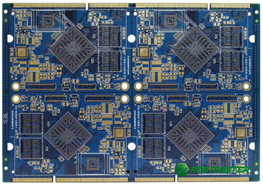
▲ PCB panel with V-CUT
V-CUT Design Guidelines
l Clearance requirement: The centerline of the V-score must be at least 0.4 mm away from traces, pads, and copper pours to avoid circuit damage or pad cracking caused by depaneling stress.
l Board thickness limit: Suitable for board thicknesses ≤ 3.5 mm. For ultra-thin boards (< 0.6 mm), a composite support design should be considered to prevent inner-layer cracking.
l Keepout zone: Maintain a component keepout area of at least 1 mm on both sides of the V-score line to prevent automated depaneling from damaging components—especially sensitive parts such as BGAs.
l Narrow connection sections: If a connecting section is less than 2 mm wide, it is recommended to open the gap to 1.6–2 mm and switch to routed edge processing instead of V-CUT to prevent breakage during depaneling.
l Scoring depth: Control the V-score depth to 1/3 to 1/2 of the board thickness, so the board can be easily separated without excessive burrs, while also preventing premature breakage during production.
2. Mouse Bite Panelization: The Best Choice for Irregular Board Shapes
Mouse bites are ideal for round, polygonal, or otherwise irregular board outlines. They offer excellent flexibility and can significantly reduce the risk of depaneling stress damaging precision edge components.
However, the design parameters must be accurate—otherwise you may encounter issues such as break-off failure, burrs, or edge chipping.
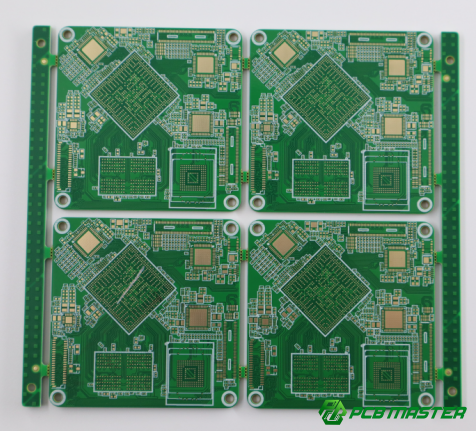
▲ PCB panel with mouse bites
Standard Mouse Bite Parameters
l Hole size and quantity: Each tab should typically use 5–8 non-plated holes with a 0.5 mm diameter. Fewer than 5 holes may result in insufficient mechanical strength and premature breakage during fabrication or depaneling.
l Hole spacing: Edge-to-edge spacing between holes should be 0.35–0.4 mm, with an absolute minimum of 0.3 mm. For thinner boards, the spacing should be increased appropriately to improve tab strength.
l Number of tabs: For board widths within 30 mm, use at least 2 symmetrically placed tabs. Add one additional tab every 50–60 mm to ensure even force distribution and reduce the risk of deformation during depaneling.
l Placement considerations: Mouse bite tabs should be placed on the centerline of the panel frame or extend about 1/3 into the board area. Avoid vias, traces, mounting holes, and protruding components. The hole edge should be at least 0.5 mm from the board edge.
l Critical warning: Maintain at least 0.35 mm clearance between mouse bite holes and inner-layer high-speed signal traces (0.4 mm recommended) to prevent burrs from penetrating insulation layers and causing shorts—especially in high-frequency or high-speed PCBs.
3. Hollow Connection Tabs (Bridging): The Only Option for Castellated-Hole Boards
For module boards with castellated holes on all four sides (such as Bluetooth modules), V-CUT and mouse bites are not suitable.
In these cases, the only viable option is hollow connection tabs (bridging tabs).
However, special care must be taken to manage stress concentration.
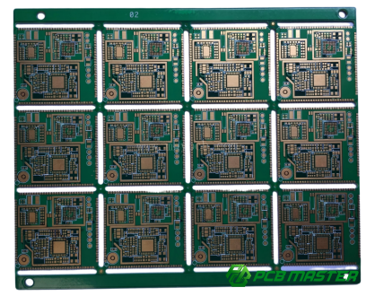
▲ PCB panel with bridge tabs
Design Guidelines
l The tab width is typically less than 2 mm, with a moderate length to ensure:
- it can be easily cut during depaneling, and
- it will not break off prematurely during production.
l After depaneling, small protrusions may remain on the board edge, but these are generally easier to clean up than mouse bite burrs and can usually be smoothed with light sanding.
l Important: Bridging tabs concentrate stress. Avoid placing them near sensitive components, as depaneling stress may cause component detachment or pad cracking.
Additional Recommendation
Try to avoid using simple direct bridges (i.e., connecting boards with a thin strip of copper only).
This method can leave behind copper remnants or cause circuit damage during separation, and it is especially unsuitable for high-frequency or high-speed PCBs.
Process Rails and Auxiliary Features
No matter which panelization method you choose, process rails, tooling holes, and fiducials are all critical. These auxiliary features directly affect SMT placement accuracy and production efficiency.
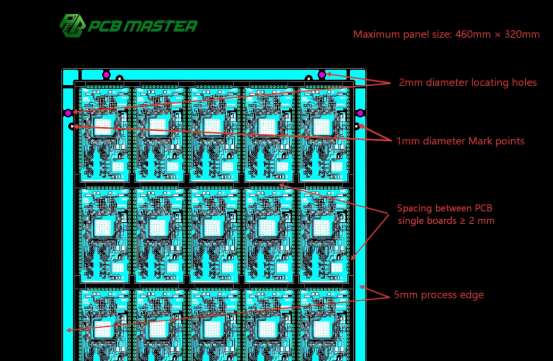
l Process rail width: It is recommended to add 5 mm process rails on two symmetrical sides or all four sides (minimum ≥ 3 mm) for SMT conveyor transport and positioning. If components are located within 3 mm of the board edge, process rails are mandatory to prevent damage from machine clamping during placement.
l Tooling holes: Include at least 4 tooling holes with a 2 mm diameter on the process rails. One of them should be offset by 5 mm to prevent reverse loading and ensure accurate SMT positioning.
l Fiducials (Mark points): The process rail should include 1 mm diameter fiducials for pick-and-place vision alignment. Additional fiducials may be added near each sub-board to identify bad units more efficiently and improve production throughput.
l Panel size control: It is recommended to keep the finished panel size around 150 × 200 mm per side range. Oversized panels are more prone to warpage, which affects placement accuracy and depaneling quality. Panel size should also be matched to:
- the PCB fabricator’s standard production panel sizes (commonly 500 × 600 mm or 450 × 600 mm), and
- the SMT line conveyor width (typically 50–400 mm).
l Panel spacing: For V-CUT, the spacing is typically ≥ 0.35–0.4 mm, while still ensuring no burrs or residual material after separation. For mouse bite panels, the spacing should be ≥ 2 mm to allow router tool access.
l Consistent process parameters: If the panel includes different PCB models or thicknesses, all unit boards should still maintain consistent fabrication parameters—such as board thickness, copper weight, solder mask, and hole sizes—to avoid yield loss caused by process mismatches.
Depaneling: How to “Break Up” Gently
After SMT assembly, the depaneling step determines the final reliability of the product.
Each depaneling method has its own pros and cons, and the best choice depends on:
l board geometry,
l production volume, and
l component sensitivity.
Based on PCBMASTER’s one-stop PCBA service experience, here is a practical breakdown:
| Depaneling Method | Best For | Pros / Cons |
| Manual breaking | Small batches, prototype validation | Pros: Simple, low cost. Cons: Stress is uncontrolled, easily damages components or cracks the PCB; not suitable for precision boards. |
| V-CUT depaneling machine | Regular rectangular boards in medium to high volume | Pros: High efficiency, clean edges. Cons: Blades require regular grinding, cutting speed must be controlled to prevent edge chipping; not suitable for irregular boards. |
| Router depaneling machine (CNC) | Mouse bite panels, irregular boards, or boards with precision edge components | Pros: High precision, very low stress, ideal for BGAs and other sensitive parts. Cons: Lower throughput and slightly higher cost. |
| Laser cutting | Ultra-precision designs, flex boards, or zero-stress requirements | Pros: Non-contact, zero stress, no burrs. Cons: Expensive equipment and lower throughput than mechanical cutting, making it less cost-effective for high-volume production. |
▲ V-score depaneling machine
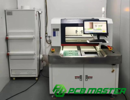
▲ CNC router depaneling machine
Common Depaneling Problems + Solutions
Many customers report issues such as PCB cracking, component detachment, or edge burrs after depaneling.
In reality, these problems can usually be avoided with proper design and handling. Based on PCBMASTER’s real-world experience, here are the most common issues and how to solve them:
Problem 1: Burrs or Edge Chipping After Depaneling
Common causes:
l Panel spacing is too small
l V-score depth is insufficient
l Incorrect depaneling method is used (e.g., forcibly snapping an irregular board by hand)
l The base material is brittle (such as thick FR-4)
Solutions:
l Reserve sufficient spacing during panel design
l Control V-score depth to 1/3–1/2 of the board thickness
l For irregular boards or thick boards (board thickness ≥ 2.0 mm), avoid manual snapping and use a router depaneling machine
l Lightly sand the edge after separation if needed
l Prefer tougher laminate materials when possible
l For brittle materials such as ceramic substrates, use mouse bites + routed depaneling
Problem 2: Components Falling Off or Pads Cracking After Depaneling
Common causes:
l Excessive force during depaneling
l Stress concentration near connection tabs
l Components placed too close to connection areas
l Depaneling performed before solder joints are fully stabilized
Solutions:
l Depanel gently and use proper depaneling equipment to distribute stress
l In panel design, keep components away from connection areas
l Maintain at least 1 mm clearance between pads and connection points
l After SMT, wait until the solder has fully solidified (allow the reflowed assembly to cool to room temperature) before depaneling
Problem 3: PCB Warpage or Deformation After Depaneling
Common causes:
l Uneven force during depaneling
l Oversized panels
l Inconsistent board thickness
l No flattening treatment after depaneling
Solutions:
l Apply force evenly during depaneling
l Use a section-by-section depaneling approach
l Avoid overly large panel sizes; for larger-volume orders, split the job into multiple smaller panels
l After depaneling, place the PCB on a flat work surface and cover it with a steel plate for 1–2 hours to relieve stress and correct deformation
If the customer does not have depaneling equipment or is concerned about depaneling risk, PCBMASTER can also provide a “panelized production + depanelized delivery” value-added service.
Using dedicated depaneling equipment, we ensure:
l no board damage,
l no burrs, and
l direct compatibility with subsequent assembly.
This creates a true “ready-to-use out-of-the-box” panelized delivery experience.
Common Misconceptions About Panelized vs. Individual Delivery: Avoid These and Save Money
Based on years of customer service experience, we’ve found that many customers fall into a few common traps when choosing delivery formats and handling downstream processes. These mistakes often lead to higher costs and longer lead times.
Be sure to avoid these three major misconceptions:
Myth #1: “The more units per panel, the cheaper it gets.”
Panel quantity must be planned rationally based on board geometry and equipment capability. Blindly maximizing units per panel can make the panel oversized, complicate SMT alignment, and actually increase cost and rework rates.
Myth #2: “Individual board delivery is always easier.”
Small individual boards (< 50 × 50 mm) often cannot run properly on a standard SMT line and may require custom carriers or fixtures. This increases both assembly cost and turnaround time, making panelized delivery the more efficient option.
Myth #3: “You can just snap the boards apart however you want.”
Improper depaneling can damage the PCB or cause components to fall off. The rework cost afterward is usually far higher than the time saved by careless separation. Standardized depaneling procedures—or factory depaneling services—are strongly recommended.
PCBMASTER’s Service Commitment
Panelization design is not just a technical task—it’s an experience-driven discipline.
With years of deep expertise in the PCB industry, PCBMASTER offers a seasoned engineering team and full-process one-stop support to help you reduce risk, lower cost, and improve efficiency.
Our Commitment to You
l Free panelization design review
We help optimize panel size, connection methods, process rails, tooling holes, and other design details—identifying potential issues early and ensuring the panel design is fully compatible with SMT production.
l One-stop manufacturing service
From PCB fabrication to SMT assembly, depaneling, and inspection, we manage the entire process to ensure panel quality and precision—enabling a seamless transition from design to volume production.
l Professional technical support
Whether you’re in the design stage or already in mass production, we’re ready to answer questions about panel design, depaneling, delivery format selection, and more, with customized one-on-one solutions.
l Value-added depaneling service
For customers without depaneling equipment—or those concerned about depaneling risks—we offer panel depaneling + inspection services to ensure the delivered PCBs are burr-free, damage-free, and ready for immediate use.
Conclusion
Choosing between panelized PCB delivery and individual board delivery is not just a manufacturing preference—it directly affects cost, SMT efficiency, depaneling safety, and overall product reliability. For small boards and SMT-driven projects, panelization often provides better production efficiency and lower total cost. However, the right approach depends on your board size, shape, component placement, assembly process, and depaneling method.
A well-designed PCB panel should support not only fabrication, but also assembly, inspection, testing, and safe separation after reflow. By selecting the proper panelization method—whether V-score, mouse bites, or bridge tabs—and planning rails, fiducials, and clearances correctly, you can avoid costly rework and improve manufacturing yield.
If you are unsure which delivery method is best for your project, working with an experienced PCB and PCBA partner like PCBMASTER can help you optimize the design early and reduce risk before production begins.
FAQs
1. Is PCB panelization required for SMT assembly?
Not always, but it is often strongly recommended for small or lightweight boards.
Many SMT assembly lines cannot reliably handle very small PCBs without rails, fixtures, or panel support. If your board is difficult to convey, align, or depanel safely, panelization can improve placement stability, reduce handling errors, and lower total assembly cost.
2. What is the best PCB panel size for automated assembly?
There is no single universal panel size, but most PCB assembly providers prefer a panel that fits standard SMT conveyor and handling systems.
A practical panel should be large enough for stable transport, fiducial recognition, and efficient placement, but not so large that it creates warpage, handling difficulty, or poor material utilization. The ideal size depends on your board dimensions, component density, and your supplier’s equipment limits.
3. How much does PCB panelization reduce assembly cost?
The savings can be significant, especially for small boards.
While panelization may slightly increase bare board area because of rails and breakaway tabs, it often reduces overall manufacturing cost by improving SMT throughput, minimizing fixture requirements, and lowering manual handling time. For compact boards or medium-volume builds, the total cost savings can be substantial compared with ordering fully separated single boards.
4. What is the difference between V-score and mouse bites in PCB panelization?
V-score (V-cut) is usually preferred for straight-edged rectangular boards because it enables fast, clean, and efficient depaneling.
Mouse bites are better for irregular board shapes, rounded outlines, or designs that need more flexible breakaway tab placement.
The right choice depends on your board shape, edge component clearance, material thickness, and how the boards will be separated after assembly.
5. How close can components be to the PCB edge in a panelized design?
That depends on the panel method and the depaneling process, but components placed too close to the board edge can be at risk during SMT handling and separation.
If components are near breakaway tabs, V-score lines, or process rails, they may be exposed to mechanical stress, tool interference, or conveyor clamping pressure. A design review with both the PCB fabricator and the assembler is the best way to confirm safe edge clearance before production.
6. Can a PCB manufacturer deliver panelized boards and depanel them before shipping?
Yes, many PCB and PCBA suppliers can do that.
Some customers want panelized production for efficient SMT assembly but still prefer individual boards for final delivery. In that case, the supplier can fabricate and assemble the boards in panel form, then use professional depaneling equipment before shipment. This is often a good option when the customer does not have in-house depaneling tools or wants to reduce handling risk.
7. What is the minimum PCB size for SMT without panelization?
There is no universal minimum size because it depends on the SMT line, board thickness, component layout, and whether fixtures are available.
However, very small PCBs often become difficult to transport and align consistently as standalone units. If a board is too small, too light, or has edge components that interfere with handling, panelization is usually the safer and more cost-effective solution.
8. Is panelized PCB delivery better for prototype builds or only for mass production?
Panelization is not just for mass production.
It is often useful in prototype and low-volume builds as well—especially when the board is small, irregularly shaped, or intended for SMT assembly. In many cases, panelization during prototyping helps validate manufacturability early and prevents surprises when moving into pilot runs or full production.
9. Can poor PCB panel design cause assembly defects?
Absolutely.
A poorly designed panel can lead to alignment problems, warpage, inaccurate pick-and-place, soldering issues, depaneling damage, and even lower inspection yield. Panel design is not just a fabrication concern—it directly affects assembly performance, product reliability, and total manufacturing efficiency.
10. Should I let my PCB supplier design the panel, or should I create it myself?
If you already understand your assembler’s requirements, you can provide your own panel design.
However, many buyers prefer to send the single-board design first and ask the supplier to recommend or optimize the panel layout based on fabrication capability, SMT line constraints, and depaneling method. This often reduces engineering risk and helps ensure the panel is actually production-ready—not just manufacturable on paper.
Author Bio
Hi, I'm Carol, the Overseas Marketing Manager at PCBMASTER, where I focus on expanding international markets and researching PCB and PCBA solutions. Since 2020, I've been deeply involved in helping our company collaborate with global clients, addressing their technical and production needs in the PCB and PCBA sectors. Over these years, I've gained extensive experience and developed a deeper understanding of industry trends, challenges, and technological innovations.
Outside of work, I'm passionate about writing and enjoy sharing industry insights, market developments, and practical tips through my blog. I hope my posts can help you better understand the PCB and PCBA industries and maybe even offer some valuable takeaways. Of course, if you have any thoughts or questions, feel free to leave a comment below—I'd love to hear from you and discuss further!

