


Understanding PCB Board Warping: Key Causes and Prevention Tips
A perfectly flat PCB is essential for high-quality manufacturing, yet warping remains one of the most common and disruptive issues in the industry. Whether it's a minor distortion or a severe twist, PCB warping can impact everything from soldering to assembly, jeopardizing both functionality and reliability. Understanding why warping occurs and how to prevent it is crucial for any electronics manufacturer. Let’s dive into the root causes of PCB warping and explore effective strategies to tackle this issue before it affects your products.
What is PCB Warping?
PCB warping refers to the deformation of a printed circuit board (PCB) that occurs when it no longer remains flat, deviating from its original design specifications. This bending or twisting can happen after the PCB is removed from its manufacturing environment, such as the pressing or cooling process. PCB warping can result in significant issues during assembly and soldering, affecting the overall functionality of the final product. This type of deformation typically occurs due to an imbalance of stress within the layers of the PCB, leading to uneven shrinking or expansion.
In simple terms, PCB warping means the board gets bent or twisted in ways it wasn't meant to, which can make it hard to work with during the assembly or soldering process. Warping can cause misalignment of components and lead to poor soldering connections, which could eventually result in product failures.
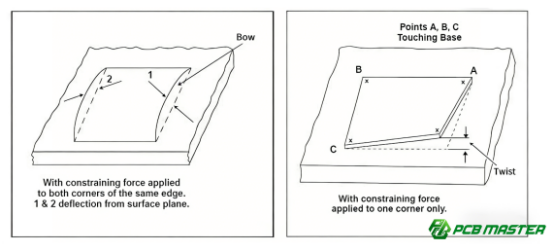
There are two main types of PCB warping:
l Bow (Concave or Convex): This type of warping causes the PCB to curve like a bowl or an arch. The four corners of the PCB remain at the same plane, while the center either rises or sinks. This is the most common type of PCB warping. For example, if you think of a concave bowl, the middle area bows inward, and when it's convex, the middle area bulges outward. Both can cause issues when placing components or soldering.
l Twist (Torsion): This type of warping causes the PCB to twist, making one corner of the board higher or lower than the others. It’s often compared to the shape of a twisted piece of dough or a pretzel. This kind of distortion can be more problematic than bowing because it can affect the alignment of the PCB when it’s inserted into a machine for further processing, like testing or assembly.
In summary, bowing makes the PCB curve, while twisting causes the board to rotate or skew at one end, making it harder to handle or assemble accurately.
Why Do PCBs Warp?
PCBs warp due to the mismatch in the thermal expansion rates of the materials used, uneven stresses during manufacturing, and poor design choices, such as asymmetric layer stacking or uneven copper distribution.
Material Properties
PCBs warp primarily due to the different materials used in their construction, especially the mismatch in their Coefficient of Thermal Expansion (CTE). CTE is a measure of how much a material expands or contracts when exposed to temperature changes. When the materials used in a PCB expand or contract at different rates, internal stress builds up, causing warping.
l Fiberglass vs. Resin: The core of most PCBs is made from fiberglass cloth (like FR-4), which has a low CTE in the X-Y directions. The resin (a plastic material) used in the PCB has a higher CTE in the Z-axis (vertical direction). When the PCB heats up or cools down, these materials expand or shrink at different rates, leading to stress and deformation.
l Copper Foil: Copper, used for electrical connections, has a different CTE than both fiberglass and resin. When the PCB undergoes temperature changes, the copper foils expand or contract at a different rate than the core materials, contributing to warping.
In simple terms, when the materials of the PCB don't shrink or expand evenly, they cause the board to bend or twist. This is the main reason why warping often happens during manufacturing or when the PCB is exposed to heat.
Manufacturing Process Stresses
The manufacturing process plays a significant role in PCB warping. Certain steps, especially those involving temperature changes, can induce stresses that lead to deformation.
l Pressing Process: The temperature during the pressing stage can cause uneven shrinkage or expansion of the PCB layers. If the temperature rises or falls too quickly, some layers may contract or expand more than others, creating internal stresses. This leads to the board bending or twisting.
l Soldering and Reflow Soldering: The process of soldering and reflow soldering involves heating the PCB to high temperatures to melt solder. As the board cools after heating, the different materials in the PCB cool at different rates, causing them to contract unevenly. This contraction can cause the PCB to warp.
For example, during reflow soldering, the board is heated to around 250°C. When it cools, the different materials in the PCB shrink at different rates, leading to stress and possible warping.
Design Factors
Design decisions can also contribute to PCB warping. Poor design choices in the PCB's layout can cause uneven stresses that lead to warping.
l Asymmetric Layer Stacking: If the layers in a multi-layer PCB are not arranged symmetrically, the PCB will be prone to warping. For example, if the copper foil is thicker on one side of the board than the other, the board will experience uneven shrinkage during the cooling process, causing it to bend.
l Uneven Copper Distribution: If one side of the PCB has a much larger copper area than the other, it can cause an imbalance. For example, a PCB with large copper pads on one side and small traces on the other will warp because the side with the larger copper area will shrink more, creating an uneven stress across the board.
In simpler terms, if the board's internal structure isn't balanced, it will be more likely to warp, especially during the cooling or heating stages.
How Does PCB Warping Affect the Product?
PCB warping affects the product by causing difficulties in surface mounting, soldering, component insertion, testing, and final assembly, while also increasing the risk of long-term reliability issues like copper trace cracking and delamination.
Surface Mounting Difficulties
PCB warping can make it difficult to accurately apply solder paste and mount components during the surface-mount technology (SMT) process. When a PCB is not flat, the stencil used for solder paste printing may create uneven layers of paste, leading to inconsistent solder joints. Additionally, warped boards cause issues during component placement. The vacuum nozzles used to pick up and place components may struggle to make secure contact with the board, leading to misalignment or failure to properly place components. This can result in faulty solder joints or components not being attached to the board at all.
For example, if a board bows, the solder paste in the center may be thicker than at the edges, causing components to float or tilt, which can impact the performance and reliability of the final product.
Soldering Issues
Warping significantly impacts soldering processes, particularly during reflow soldering. During reflow, the PCB is heated, causing it to expand and contract. If the board is already warped, the heat can further distort it, leading to issues like cold solder joints, bridging, or soldering voids. A cold solder joint occurs when the solder does not properly melt and bond with the component lead or PCB pad, causing poor electrical connections. Solder bridges occur when excessive solder connects two or more pads, creating short circuits.
For example, if a warped PCB goes through reflow soldering, the components might shift, and solder may spread to unintended areas, causing short circuits or weak connections that can affect the product's functionality.
Difficulties with Through-Hole Component Insertion
Inserting through-hole components into a warped PCB is a challenging task. The holes for the components may no longer align properly with the PCB's inner layers due to warping, causing difficulty during assembly. If the board is twisted, one corner may be higher than the rest, making it impossible for the component pins to fit correctly into the holes. This misalignment can lead to mechanical stress during the insertion process, potentially damaging both the component and the PCB.
In practical terms, this could mean that even if the components are inserted, they may not be properly aligned, leading to poor electrical connections or difficulty securing the component in place.
Testing and Assembly Problems
l Testing: During automated optical inspection (AOI) or electrical testing, warping can cause problems with the probe’s alignment. If the PCB is not flat, the probes may not make consistent or accurate contact with the test pads, leading to false readings or failed tests. This could result in defective PCBs being sent through the production process, impacting product quality.
l Final Assembly: In the final product assembly, warped PCBs might not sit properly in their designated mounting positions inside the casing or device. This can cause stress on the components and lead to misalignment. Over time, this could also cause mechanical stress on connectors or lead to product malfunctions.
For example, a warped PCB might not fit snugly into a device's frame, causing it to shift, which might lead to loose connections or broken parts.
Long-Term Reliability Risks
Long-term reliability of a PCB can be significantly impacted by warping. The internal stresses caused by warping, especially if the PCB is forcefully straightened during assembly, can lead to the cracking of copper traces, delamination of layers, and cracking of vias (the holes that connect different layers of the PCB). These issues can compromise the integrity of the PCB over time, leading to eventual failure of the circuit. Additionally, the uneven stress might cause micro-cracks in the PCB material, which can grow over time and cause the board to fail under normal operating conditions.
For example, a PCB that is consistently exposed to bending or stress might develop cracks in the copper or internal layers, causing intermittent failures, shorts, or complete board failure, which could affect the product's lifetime.
How to Measure and Evaluate PCB Warping?
PCB warping can be measured using the IPC-TM-650 2.4.22 method or by calculating the warping degree using the formula (Maximum Deformation Height / Diagonal Length of the Board) × 100%, with tools like specialized warping gauges or pin gauges to measure height variations and gaps.
Common Measurement Standards
To measure PCB warping accurately, the industry relies on established standards to ensure consistent and reliable results.
l IPC-TM-650 2.4.22 Method: This is a commonly used standard to assess PCB warping. It involves a process where the PCB is placed on a flat surface, and the amount of deformation is measured by observing the difference in height between the highest and lowest points of the board. This method helps ensure that warping is evaluated in a standardized way across different boards and manufacturers.
l Formula for Warping Degree: The most straightforward way to calculate warping is by using the following formula:
Warping Degree = (Maximum Deformation Height / Diagonal Length of the Board) × 100%.
This formula measures the amount of deformation as a percentage of the board’s diagonal length. A larger deformation height compared to the diagonal length indicates more severe warping.
For example, if a board has a maximum deformation height of 1 mm and the diagonal length of the board is 100 mm, the warping degree would be 1%. This calculation provides a simple, quantifiable way to evaluate warping.
Measuring Tools Used
There are different tools available to help measure PCB warping accurately, ranging from basic methods to more advanced equipment.
l Warping Measurement Gauge: A specialized warping gauge is designed to measure the height differences between the highest and lowest points of the PCB. This tool typically uses a set of probes or a flat platform where the PCB is placed, and the height variations are measured with precision. This tool is commonly used for more accurate and consistent results.
l Pin Gauge for Maximum Gap Measurement: Another way to measure PCB warping is by using a pin gauge. This tool involves placing the PCB on a flat surface and using the pin gauge to measure the maximum gap between the board and the flat surface. The largest gap detected by the pin gauge represents the degree of warping. Pin gauges are especially useful when trying to detect localized warping or twist in a PCB.
For example, if a warped board has a gap of 0.5 mm at one end, this could indicate a noticeable twist or bow that would need to be addressed before the board is used in production.
How to Prevent PCB Warping in Design?
To prevent PCB warping in design, ensure symmetric layer stacking, balance copper distribution, and select high-quality materials like high-Tg and low-CTE laminates.
Symmetric Design
One of the most effective ways to prevent PCB warping is to ensure symmetric design. This means that the layers within the PCB, including the core material (the fiberglass or resin) and the copper layers, should be evenly distributed along the Z-axis (the vertical direction). By designing a balanced stack-up where the materials on the top and bottom of the PCB are symmetrical, internal stresses caused by temperature changes can be minimized. For example, if the copper foil on the top and bottom layers is of equal thickness and the inner core materials are also symmetrically placed, the PCB will be less likely to warp during manufacturing processes like pressing or cooling.
A practical example would be using a 4-layer PCB where the copper thickness on the top and bottom layers is matched, and the core and pre-preg (semi-cured resin sheets) layers are placed symmetrically. This balance helps prevent one side from contracting or expanding more than the other, which would lead to warping.
Balanced Copper Area
Balanced copper area is another crucial design consideration to avoid warping. If one side of the PCB has significantly more copper than the other (for example, large copper pads or traces), it can cause uneven contraction and expansion during manufacturing processes. When the copper on one side is removed or etched away, the difference in thermal shrinkage between the copper-heavy and copper-light sides can cause the board to bow or twist.
To address this, designers often add balance copper to areas with less copper. This "balancing" copper is non-functional and is placed specifically to reduce warping. For instance, in multi-layer PCBs, additional copper might be added to the inner layers to match the copper area on the outer layers. This design practice ensures that the board experiences even thermal expansion, preventing deformation.
For example, in a PCB with a large copper pour on one layer, a designer may add small copper pads or traces to the opposite layer to balance the thermal forces, preventing the board from warping.
Choosing High-Quality Materials
Selecting high-quality materials is essential in preventing PCB warping. The most important materials to consider are the high-Tg (glass transition temperature) and low-CTE (coefficient of thermal expansion) substrates. High-Tg materials have better heat resistance, making them less likely to soften or deform under high temperatures. This is especially important in modern electronics where lead-free soldering processes involve higher temperatures.
Using low-CTE materials helps minimize the mismatch between the PCB's different materials. Low-CTE materials expand and contract less with temperature changes, reducing internal stress. Additionally, choosing high-reliability copper-clad laminates can improve the overall stability of the PCB, ensuring that it maintains its shape during the manufacturing and soldering processes.
For example, if a PCB is designed for a high-temperature application (such as automotive or industrial electronics), choosing a high-Tg laminate will prevent the board from warping during the reflow soldering process or during extended use in high-heat environments.
How to Prevent PCB Warping During Manufacturing?
To prevent PCB warping during manufacturing, optimize the lamination process with controlled heating and cooling, pre-bake the board to release internal stress, use fixtures during reflow soldering to maintain flatness, and ensure even cooling using cold pressing or cooling racks.
Optimize the Lamination Process
During the PCB lamination process, it is critical to control the heating and cooling rates to avoid warping. The temperature increase and decrease should follow a controlled ramp-up and ramp-down curve. Rapid heating or cooling can cause uneven expansion or contraction, creating internal stresses that lead to warping. By using a gradual temperature curve, the resin layers inside the PCB have time to flow properly and bond, which reduces the risk of distortion.
Additionally, the resin flow and slow curing are important factors in stress relief. If the resin does not flow properly or cure too quickly, it can trap stress within the board, causing deformation. A controlled curing process allows the resin to fully settle and cure evenly, helping prevent the internal stresses that lead to warping.
For example, if the temperature curve in the lamination process is too steep, it could cause the PCB to expand unevenly, resulting in bowing or twisting. Therefore, a careful balance of heating and cooling is essential.
Pre-Baking the PCB
Pre-baking the PCB before critical processes is another way to release internal stresses and prevent warping. Baking the board at a controlled temperature prior to processes like lamination, soldering, or coating helps to eliminate any trapped moisture and residual stresses from earlier steps. This pre-baking step allows the materials in the PCB to stabilize and prevents them from deforming during subsequent high-temperature processes.
For instance, if a PCB undergoes pre-baking before reflow soldering, it ensures that any moisture trapped in the PCB layers is evaporated, reducing the risk of expansion during heating. This step can improve the overall dimensional stability of the board.
Using Fixtures During Reflow Soldering
During high-temperature processes like reflow soldering, using fixtures such as jigs, clamps, or trays is crucial for controlling PCB warping. These fixtures are designed to hold the PCB flat and evenly distribute pressure across the board, limiting the risk of deformation while the board is exposed to the heat of the reflow oven.
For example, a reflow oven that doesn’t use appropriate fixtures may cause the PCB to bow or twist during the soldering process, particularly if one side of the board heats up faster than the other. Using a tray or fixture ensures that the board remains level, preventing uneven thermal expansion and warping.
Cooling and Shaping
Once the PCB has gone through high-temperature processes like lamination or reflow soldering, it is important to cool the board gradually and evenly. Cold pressing or using cooling racks helps to maintain an even temperature distribution during cooling, ensuring that the PCB does not warp due to uneven cooling rates.
For example, a cooling press applies gentle pressure to the PCB as it cools, which helps prevent the board from warping by ensuring uniform contraction. This step is particularly important after processes like reflow soldering, where temperature differences between the top and bottom layers of the PCB can cause warping if not properly managed.
How to Reduce PCB Warping Through Post-Processing?
PCB warping can be reduced through post-processing by using a cold press for even cooling and applying forced straightening combined with stress relief to release internal stresses.
Cooling and Shaping with Pressing
One of the most effective ways to reduce PCB warping after the lamination process is cooling and shaping the board evenly. This is often done by using a cold press after the PCB exits the lamination machine. The cold press applies uniform pressure while the board cools, ensuring that the temperature drops consistently across the entire PCB. This helps to prevent one side from contracting faster than the other, which could otherwise cause warping.
For example, if a PCB has been exposed to high heat during the lamination process, it might expand or bow in certain areas. By using a cold press, manufacturers can flatten the PCB by applying gentle pressure, which allows it to cool in a controlled manner and reduces the chances of bowing or twisting.
Forced Straightening and Stress Relief
Sometimes, PCB warping can be too severe for cooling alone to fix. In these cases, forced straightening is employed to manually or mechanically flatten the board. This process involves applying external pressure to the warped PCB to reshape it. After this, stress relief is crucial. By gently heating the PCB and allowing it to cool slowly, internal stresses that caused the warping are gradually released.
For example, if a board has a significant twist or bow after the pressing process, manufacturers can use a stress relief oven to reheat and slowly cool the PCB. This step helps release trapped stress, preventing future warping and ensuring that the PCB stays flat.
Common PCB Warping Misconceptions
Common misconceptions about PCB warping include underestimating the importance of design symmetry, ignoring material properties like CTE mismatch, and relying solely on post-processing fixes to correct warping issues.
Misconception 1: Believing that Design Doesn't Matter
Many people believe that PCB design is not a key factor in preventing warping. However, poor design choices, especially asymmetric designs, can lead to significant warping problems. When the copper layers and other materials are not symmetrically arranged along the Z-axis, internal stresses can build up during the manufacturing process, leading to deformation. For example, if the top and bottom copper layers are not balanced in terms of thickness or distribution, the PCB may warp because one side will expand or contract differently than the other. Properly designing the PCB with symmetrical layering and balanced copper distribution is crucial in preventing such issues.
For instance, in multi-layer boards, if the inner core and pre-preg layers are not properly balanced, the PCB may bow or twist during cooling after lamination. Symmetry is essential for keeping the PCB flat throughout its manufacturing process.
Misconception 2: Ignoring Material Properties
Another common misconception is overlooking the material properties of the PCB, particularly the mismatch in CTE (Coefficient of Thermal Expansion) between the different materials used. CTE determines how much a material expands or contracts when subjected to heat. If the CTE values of the core material (like fiberglass or resin) and the copper layers are mismatched, warping is almost inevitable. This is because when the PCB is heated during processes like reflow soldering, the different materials expand at different rates, causing internal stresses that lead to warping.
For example, FR4 (a common PCB material) has a low CTE in the X and Y directions, while the resin has a higher CTE in the Z direction. If these materials are not properly matched or balanced, the PCB will warp due to the internal stress caused by differing expansion rates.
Misconception 3: Relying Solely on Post-Processing Fixes
A third misconception is that post-processing techniques like cold pressing or stress relief can fix all warping issues. While these methods can help reduce some warping after the PCB is manufactured, they have limitations and cannot fully correct severe warping caused by poor design or material selection. In many cases, these fixes are not enough to achieve the desired flatness, and warping may still occur.
For example, using a cold press after lamination can help smooth out minor deformations, but it cannot correct a poorly designed PCB that has severe asymmetry or material mismatches. Relying on post-processing alone can lead to a high failure rate, as it doesn’t address the root causes of warping.
Conclusion
Preventing and addressing PCB warping requires a comprehensive approach that spans design, material selection, and manufacturing processes. By understanding the factors that lead to warping—such as asymmetric designs, material mismatches, and reliance on post-processing fixes—you can avoid costly mistakes and ensure a more reliable end product. Whether you’re designing from scratch or facing challenges in production, it’s essential to partner with an experienced supplier who understands these complexities.
That’s where PCBMASTER comes in. As a trusted and seasoned PCB and PCBA supplier, PCBMASTER is committed to providing high-quality, reliable products designed to meet your exact specifications and manufacturing needs. With years of expertise in the field, we ensure that your PCBs are engineered to minimize warping risks, resulting in better performance and greater long-term reliability.
FAQs
Can PCB warping be completely avoided?
While it is impossible to completely eliminate the possibility of PCB warping, significant measures can be taken to minimize its occurrence. By focusing on optimizing the design (ensuring symmetry in layer stacking), selecting the right materials (such as high-Tg and low-CTE laminates), and controlling the manufacturing processes (such as managing the heating and cooling rates during lamination and reflow soldering), the risk of warping can be greatly reduced. These strategies help ensure that the board maintains its flatness throughout its production and usage.
How does PCB warping affect soldering processes?
Warping can significantly impact the quality of solder joints during processes like reflow soldering. When a PCB is warped, it causes uneven contact between the PCB surface and the components during soldering, leading to issues such as cold solder joints, solder bridges, or voids in the solder. This occurs because the board may not be completely flat, causing the solder to flow unevenly or not adhere properly to the pads and leads. Warping also increases the chances of thermal mismatch, where components and solder don’t expand or contract uniformly, resulting in weak or defective connections.
How do you choose the right materials to avoid warping issues?
Selecting the right materials is crucial to minimizing warping. Materials with a high glass transition temperature (high-Tg), such as certain laminates, offer better resistance to heat and thermal cycling, making them less prone to warping during soldering or high-temperature operations. Additionally, low-CTE (coefficient of thermal expansion) materials, which expand and contract less under temperature changes, should be used. This reduces the stress caused by mismatched thermal expansions between the copper layers and the core material, which is a primary cause of warping. By choosing materials that balance thermal expansion properties, the likelihood of warping is reduced significantly.
How can asymmetric layer stacking be avoided in design?
Asymmetric layer stacking in PCB design is one of the main contributors to warping. To avoid this, designers should ensure that the layer stack-up is symmetrical along the Z-axis. This means that the thickness of the copper layers and the placement of pre-preg (semi-cured resin) layers should be evenly distributed. For example, the inner layers of the PCB should be balanced with the outer copper layers to prevent uneven thermal expansion during heating. In multi-layer boards, it's also important to match the copper weight (thickness) on the top and bottom layers and the inner layers to achieve overall symmetry, reducing internal stresses that can lead to warping.
How can PCB warping be prevented during reflow soldering?
To prevent PCB warping during reflow soldering, fixtures or trays should be used to hold the PCB in place during the process. These fixtures prevent the board from bending or twisting under the high temperatures of the reflow oven, where the board expands due to heat. The use of fixtures ensures uniform heating, as the board remains level throughout the soldering process. This helps avoid areas where the PCB might warp due to uneven temperature exposure. Additionally, maintaining a controlled reflow temperature profile and avoiding rapid cooling or heating can further help prevent warping during the soldering process, ensuring stable and reliable solder joints.
Author Bio
Hi, I'm Carol, the Overseas Marketing Manager at PCBMASTER, where I focus on expanding international markets and researching PCB and PCBA solutions. Since 2020, I've been deeply involved in helping our company collaborate with global clients, addressing their technical and production needs in the PCB and PCBA sectors. Over these years, I've gained extensive experience and developed a deeper understanding of industry trends, challenges, and technological innovations.
Outside of work, I'm passionate about writing and enjoy sharing industry insights, market developments, and practical tips through my blog. I hope my posts can help you better understand the PCB and PCBA industries and maybe even offer some valuable takeaways. Of course, if you have any thoughts or questions, feel free to leave a comment below—I'd love to hear from you and discuss further!

