


Precision PCB Routing for High-Performance Circuits: Techniques for Accurate Board Fabrication
High-performance circuits power everything from smartphones to advanced medical devices, where precision is crucial for reliability. Even the smallest misstep in PCB routing, like incorrect trace width or poor via placement, can lead to signal interference or failure. As electronics become more compact and complex, achieving accurate routing has never been more important.
This article explores the essential techniques for precise PCB routing, focusing on methods that ensure your designs perform flawlessly. Whether it’s fine line routing, impedance control, or optimal layer stack-up, mastering these techniques will help you build circuits that meet the highest standards of quality and performance. Let’s dive into the world of precision routing and see how these strategies can elevate your designs.
What is Precision PCB Routing and Why is It Important for High-Performance Circuits?
Precision PCB routing ensures accurate placement of traces, vias, and components, which is crucial for maintaining signal integrity, minimizing interference, and optimizing performance in high-speed, high-density circuit designs.
Definition: Precision PCB Routing Involves Accurate Placement of Traces, Vias, and Components
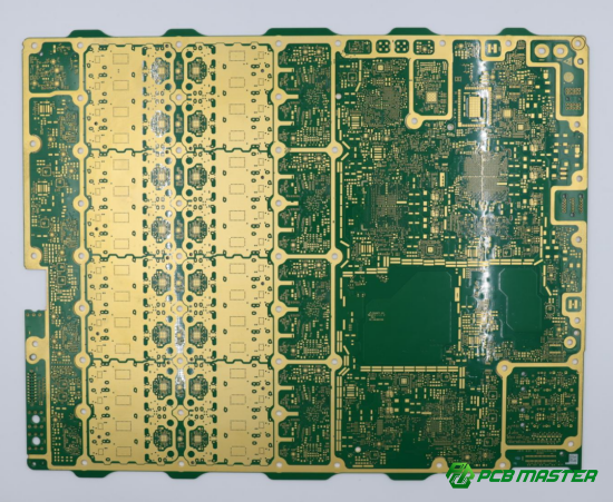
Precision PCB routing refers to the careful and accurate placement of the conductive paths (traces), holes (vias), and components on a printed circuit board (PCB). In simple terms, it’s about ensuring that the electrical connections on the board are exactly where they need to be, with very little margin for error.
Traces are the pathways that connect the different components on the PCB, such as resistors, capacitors, and microchips. Vias are tiny holes that allow electrical signals to pass between different layers of a multi-layer PCB. Components, such as chips or connectors, need to be positioned accurately to ensure the electrical connections work as intended.
Why does precision matter here? If traces are too wide or too narrow, or vias are incorrectly placed, it can cause issues like signal interference, power loss, or even complete circuit failure. Therefore, precision in PCB routing is about ensuring everything is in the right place with the correct dimensions to avoid these problems.
Why It Matters: Essential for Ensuring Signal Integrity, Minimizing Interference, and Optimizing Circuit Performance in High-Speed and High-Density Designs
Why does precision matter for high-performance circuits? High-speed circuits (like those used in smartphones, computers, or communication systems) require extremely accurate PCB routing to function properly. Even small errors in trace width, via size, or component placement can lead to performance issues, like signal degradation or electromagnetic interference (EMI).
l Signal Integrity: In high-performance circuits, the signal must travel through the PCB traces without being altered or degraded. If traces are routed inaccurately, the signals can become corrupted, leading to errors or slower performance. Proper trace width and spacing ensure the signals remain clear and accurate.
l Minimizing Interference: When PCB routing isn’t precise, electrical signals can "leak" into nearby traces, creating noise and interference. This is especially problematic in high-speed designs, where even a small amount of interference can drastically impact performance. Precision routing minimizes this risk by ensuring that signals are properly isolated and the trace layout is optimal.
l Optimizing Performance: For high-density circuits, where there are many components packed into a small space, precision routing ensures that all connections are made efficiently, without unnecessary complexity or interference. This helps maintain the reliability of the entire circuit, especially in compact or high-performance applications.
Real-Life Example
Imagine designing a smartphone circuit that processes high-speed data. The traces must be designed with very specific width and spacing to ensure signals travel quickly and without distortion. If the trace spacing is too narrow, signals could interfere with each other, causing glitches or slowdowns. Precision in routing ensures the signals are clear, and the phone works smoothly without lag or errors.
In a high-performance PCB design, controlled impedance is often used to ensure that signal speed and quality are maintained. This involves routing traces with precise width and spacing, based on the material and environmental factors, to prevent any variation in signal transmission.
Key Techniques for Precision PCB Routing
Key techniques for precision PCB routing include fine line routing, controlled impedance, accurate via and hole placement, optimized layer stack-up, and design rule checking to ensure signal integrity, space efficiency, and reliable performance in high-speed, high-density circuits.
Fine Line Routing: Minimizing Trace Width While Maintaining Signal Quality
What is Fine Line Routing?
Fine line routing involves designing PCB traces that are as narrow as possible, allowing for more compact layouts and high-density circuit designs. This technique is particularly important for high-performance circuits where space is limited, and signal integrity must be preserved.
Why Does It Matter?
By reducing the trace width, designers can fit more components onto the PCB, which is essential in modern devices like smartphones or wearable technology. However, narrowing the traces too much can lead to signal loss, increased resistance, and overheating. Therefore, it’s crucial to strike the right balance between reducing trace width and maintaining the electrical performance of the circuit.
Example:
In a smartphone PCB design, fine line routing allows the designer to fit more components in the same space, enabling a smaller, more efficient device. However, if the traces are too thin, the signals can degrade, causing performance issues like data corruption or slower processing speeds.
Controlled Impedance Routing: Ensuring Consistent Impedance for High-Frequency Applications
What is Controlled Impedance Routing?
Controlled impedance routing is a method used to maintain a consistent impedance along the PCB traces, particularly for high-frequency signals. Impedance refers to the resistance a signal encounters as it travels through the trace, and maintaining a constant value is critical for minimizing signal distortion and ensuring reliable data transmission.
Why Does It Matter?
For high-speed circuits, like those in 5G communication systems or high-speed data transmission devices, any variation in impedance can cause reflection, signal loss, or crosstalk. Precision in controlling impedance helps prevent these issues, ensuring that the signal arrives at its destination without interference.
Example:
In data centers, where high-speed communication is crucial, maintaining controlled impedance ensures that signals pass through without distortion. This is achieved by adjusting the trace width, spacing, and the PCB material type, which helps match the required impedance for high-frequency signals.
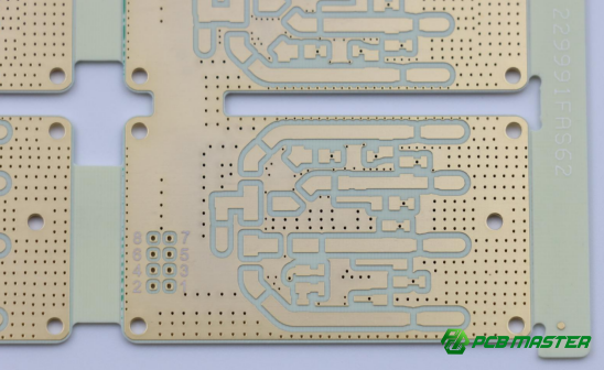
Via and Hole Placement: Accurate Placement for Signal Integrity and Space Efficiency
What is Via and Hole Placement?
Via and hole placement refers to the precise positioning of vias (small holes that connect different layers of a PCB) and other holes that support components. Correct placement is essential for maintaining signal integrity and efficient use of space on multi-layer PCBs.
Why Does It Matter?
Improper via placement can lead to signal interference, increased inductance, or unwanted capacitive effects, all of which can degrade the performance of high-speed circuits. Accurate via placement ensures that the electrical signals are routed in the shortest path possible, reducing noise and interference.
Example:
For a wearable device PCB, the placement of vias must ensure that each layer is connected without causing unnecessary noise or interference in signal paths. Strategically placed vias not only ensure better signal integrity but also help in optimizing the overall size of the circuit, making the device smaller and more efficient.
Layer Stack-Up Optimization: Efficient Use of Multi-Layer PCB Designs to Achieve Precision
What is Layer Stack-Up Optimization?
Layer stack-up optimization involves determining the most effective arrangement of layers in a multi-layer PCB. Each layer has a specific function, such as signal, power, or ground layers. Optimizing the stack-up ensures that signal traces are routed in the most efficient manner, minimizing noise and interference.
Why Does It Matter?
Multi-layer PCBs are commonly used in high-performance electronics, allowing for more complex designs with fewer physical constraints. Proper layer stack-up helps manage high-frequency signals and power distribution, preventing problems like signal crosstalk or electromagnetic interference (EMI).
Example:
In medical devices with multi-layer PCBs, a properly optimized layer stack-up allows for noise-free signal transmission and stable power distribution. The arrangement of layers ensures that sensitive signals do not interfere with noisy power or ground layers, maintaining the device's reliability.
Design Rule Checking (DRC): Automated Checks to Ensure Design Accuracy During Routing
What is Design Rule Checking (DRC)?
Design Rule Checking (DRC) is a process where PCB design software automatically checks if the design adheres to predefined rules for trace widths, component spacing, via sizes, and other important parameters. DRC ensures that the design meets manufacturing capabilities and prevents costly errors.
Why Does It Matter?
DRC helps catch potential design errors early, ensuring that the PCB can be fabricated without issues. It eliminates common mistakes like too-narrow traces, improperly spaced components, or vias that are too small, all of which could lead to functionality or performance problems during manufacturing or after assembly.
Example:
In the design of a consumer electronics PCB, DRC can detect errors such as traces that are too close to each other, which could result in shorts or signal interference. By running DRC checks before production, the designer ensures that the PCB will function as expected and be manufacturable.
Challenges in Precision PCB Routing
Challenges in precision PCB routing include tighter tolerances, manufacturing limitations like minimum trace width and via size, and balancing high-quality routing with cost constraints.
Tighter Tolerances: Increasingly Precise Requirements in Modern Designs
What are Tighter Tolerances?
Tighter tolerances refer to the increasingly narrow margins for error in modern PCB designs. As technology advances, electronic devices become smaller, more powerful, and more complex, demanding even more precise circuit board layouts. This includes smaller trace widths, narrower spacing between traces, and more exact placement of components and vias.
Why Does It Matter?
As devices become smaller and require more functionality in less space, the demand for tighter tolerances increases. For example, a mistake in trace width or component placement can lead to poor signal integrity or device malfunction, especially in high-speed applications like smartphones or medical devices. Even small errors can cause signal degradation, crosstalk, or failure to meet performance specifications.
Example:
In smartphone design, a slight misalignment of components or traces could interfere with critical components like the processor or wireless antennas, leading to a reduction in performance or connectivity issues. Designers must account for tighter tolerances to ensure the phone operates smoothly in these compact spaces.
Manufacturing Limitations: Constraints Like Minimum Trace Width and Via Size
What are Manufacturing Limitations?
Manufacturing limitations refer to the physical constraints of PCB fabrication processes, such as the minimum trace width, via size, and layer count that can be achieved. As PCB designs push for higher precision, manufacturers face challenges in maintaining quality while meeting these tiny design specifications.
Why Does It Matter?
The smaller the trace width and via size, the harder it becomes to manufacture them accurately. For instance, extremely narrow traces or very small vias may not be achievable with certain fabrication techniques, potentially compromising the design’s performance or reliability. If these constraints are not properly considered, it could lead to defects in the final product, such as short circuits or poor electrical performance.
Example:
When designing a wearable device PCB, the manufacturer may face limitations on how small the traces can be. If the traces are too thin, the circuit may fail, or the device may overheat due to insufficient power distribution. Manufacturers must ensure that their equipment can handle these precise design requirements.
Cost vs. Precision: Balancing High-Quality Routing with Cost Constraints
What is the Cost vs. Precision Challenge?
Balancing cost with precision is one of the biggest challenges in PCB routing. High-precision routing often requires advanced technology, specialized materials, and additional processing steps, which can significantly increase production costs. For many companies, striking the right balance between high-quality routing and cost-effective manufacturing is critical.
Why Does It Matter?
Precision routing might offer superior performance, but it can be more expensive due to the need for more advanced manufacturing techniques, like fine-line processing or the use of high-quality materials. On the other hand, reducing costs by using less precise methods can result in lower performance, reliability issues, or even product failure. Manufacturers and designers must find the right tradeoff to meet both performance requirements and budget constraints.
Example:
In the production of consumer electronics, companies must decide whether to use the most advanced PCB technology to ensure the highest precision or opt for a cheaper manufacturing method that may compromise performance. For instance, using high-speed materials and narrow trace widths could significantly increase costs, but it would also ensure optimal signal integrity for high-speed functions like Wi-Fi and Bluetooth.
Impact of High-Frequency Considerations on Precision Routing
High-frequency considerations, such as minimizing signal reflection and crosstalk, along with selecting the right materials and surface finishes, are essential for maintaining signal integrity and optimal performance in precision PCB routing for high-speed circuits.
Signal Reflection and Crosstalk: Strategies to Minimize Interference in High-Speed Circuits
What is Signal Reflection and Crosstalk?
Signal reflection and crosstalk are types of interference that occur in high-speed PCB designs. Signal reflection happens when an electrical signal travels along a trace and encounters an impedance mismatch, causing the signal to bounce back. Crosstalk occurs when signals from nearby traces interfere with each other, which can cause noise or errors in the transmitted data.
Why Does It Matter?
Both signal reflection and crosstalk can significantly degrade the performance of high-speed circuits, leading to data errors, slower speeds, or even circuit failure. As devices get faster and more compact, minimizing these types of interference is crucial for maintaining the reliability of high-performance electronics.
How to Minimize Signal Reflection and Crosstalk:
l Controlled Impedance Routing: Ensuring consistent impedance across all traces helps reduce reflection by matching the signal’s impedance with the trace’s impedance.
l Shielding and Spacing: Increasing the spacing between traces and adding shielding can reduce the likelihood of crosstalk by preventing signals from “leaking” into adjacent traces.
l Via Optimization: Minimizing the use of vias and keeping them as short as possible can help reduce both reflection and crosstalk by maintaining a more direct signal path.
Example:
In high-speed networking equipment, signal reflection and crosstalk can lead to lost data or transmission errors. By optimizing trace routing and maintaining controlled impedance, manufacturers ensure that signals flow clearly without interference, allowing for faster and more reliable data transmission.
Material and Surface Finish: How Material Choice and Surface Treatment Affect Precision Routing in High-Frequency Designs
What is the Impact of Material and Surface Finish on Precision Routing?
The material choice and surface finish of a PCB are critical factors in high-frequency designs. The materials used affect the electrical properties of the traces, such as signal propagation speed and impedance. Additionally, the surface finish (the outer layer of the PCB) impacts the quality of the electrical connection and affects the soldering process.
Why Does It Matter?
Certain materials, like FR4 (a standard PCB material), may not perform well at high frequencies due to signal loss or excessive resistance. High-performance PCBs often use materials like Rogers or PTFE, which offer lower signal loss and better high-frequency performance. The right surface finish, such as HASL (Hot Air Solder Leveling) or ENIG (Electroless Nickel/Immersion Gold), ensures better signal conductivity and more reliable connections for high-speed signals.
How Material and Surface Finish Affect Routing:
l Material Selection: Materials with low loss factors, such as Rogers 4003 or PTFE, are ideal for high-frequency designs because they minimize signal attenuation.
l Surface Finish: The surface finish impacts the trace's conductivity. For example, ENIG provides a smooth surface with better performance for high-frequency signals than traditional HASL.
l Dielectric Constant: The dielectric constant (a material’s ability to store electrical energy) affects the impedance of traces. Materials with consistent dielectric constants, like Rogers, help ensure stable signal transmission.
Example:
In 5G base station PCBs, using high-performance materials like Rogers RO4003C helps reduce signal loss over long distances, ensuring that the high-speed data transmission required for 5G networks is reliable. The use of a high-quality surface finish like ENIG further enhances conductivity and ensures long-lasting, efficient signal flow.
Best Practices for Achieving Accurate PCB Routing
Best practices for achieving accurate PCB routing include adhering to industry standards, testing and prototyping designs, and implementing rigorous quality control throughout the manufacturing process.
Adhering to Industry Standards: Following Established Guidelines for Routing Precision
What are Industry Standards for PCB Routing?
Industry standards for PCB routing are established guidelines and best practices that ensure PCB designs are reliable, manufacturable, and meet performance requirements. These standards include specifications for trace width, spacing, via sizes, and layer stack-up that maintain signal integrity and ensure a high-quality finished product.
Why Does It Matter?
Adhering to industry standards is essential because it helps ensure that the design will work correctly when manufactured. Following these guidelines prevents issues such as poor signal transmission, manufacturing defects, or compatibility problems with components. It also allows for easier collaboration between designers and manufacturers, as everyone follows the same set of rules.
How to Follow Industry Standards:
l IPC-2221: This standard provides general requirements for designing PCBs, focusing on trace width, spacing, and layer stack-up.
l IPC-7351: Defines the land patterns and component footprints necessary for reliable PCB designs.
l Design Rule Checks (DRC): Use software tools to automatically check designs against these standards before sending them to manufacturing.
Example:
In automotive electronics, following established standards ensures that the PCB will function reliably in extreme conditions (heat, vibration, etc.) without failure, ensuring safety and performance.
Testing and Prototyping: Verifying Routing Accuracy Through Prototype Boards and Testing Methods
What is Testing and Prototyping for PCB Routing?
Testing and prototyping involve creating a physical model of the PCB before full-scale production. This prototype allows designers to verify that the routing is accurate and the PCB performs as expected in real-world conditions.
Why Does It Matter?
Prototyping helps identify potential issues in the design that may not be obvious in software simulations. By testing the prototype, designers can verify signal integrity, check for manufacturing issues, and make adjustments before mass production begins, saving time and money.
How to Conduct Testing and Prototyping:
l Create a Prototype: Once the PCB design is complete, create a small batch of boards to test.
l Test for Signal Integrity: Use tools like an oscilloscope or TDR (Time Domain Reflectometer) to check for signal degradation, crosstalk, or other issues.
l Perform Functional Testing: Power up the prototype and check if it meets performance specifications and functions correctly.
Example:
When designing a consumer electronics product, prototyping and testing allow the designer to test signal quality and check whether the board fits within the device’s compact design. This step ensures that all connections work before mass production.
Quality Control: Implementing In-Line Inspections and Audits to Maintain Fabrication Accuracy
What is Quality Control in PCB Manufacturing?
Quality control in PCB manufacturing involves systematic processes and inspections during fabrication to ensure that the design is accurately produced and free of defects. This includes visual inspections, automated optical inspections (AOI), and electrical testing to detect issues such as short circuits, open traces, or incorrect component placements.
Why Does It Matter?
Maintaining consistent quality throughout the manufacturing process ensures that each PCB performs as expected and meets reliability standards. Without proper quality control, defects can slip through, causing faulty products, device failures, or safety hazards, especially in high-performance applications.
How to Implement Quality Control:
l Automated Optical Inspection (AOI): AOI systems automatically scan PCBs for visual defects, such as missing components or soldering issues.
l Electrical Testing (E-test): Checks the electrical connections to verify that the circuit performs correctly under power.
In-Line Inspections: Continuous checks during the manufacturing process to catch defects early.
Example:
In medical device manufacturing, stringent quality control is vital to ensure that the PCB operates reliably in sensitive environments, like heart rate monitors or infusion pumps. Regular inspections and audits prevent critical errors that could lead to device malfunction or patient harm.
Conclusion
Precision PCB routing is crucial for designing high-performance, reliable circuits that meet the increasing demands of modern electronics. Key techniques such as fine line routing, controlled impedance, accurate via placement, and adhering to industry standards ensure that your PCB designs are both functional and efficient. Additionally, thorough testing and quality control processes further guarantee that each design will perform optimally when manufactured.
The role of precision in PCB routing cannot be overstated—especially in high-speed and high-density designs, where even the smallest error can lead to significant performance issues. By focusing on these best practices, you can ensure that your circuits are both reliable and capable of handling demanding tasks.
For those looking for expert assistance in achieving high-quality PCB designs, PCBMASTER is a seasoned PCB and PCBA supplier committed to delivering top-notch products. With years of experience in the industry, PCBMASTER helps clients create precisely engineered circuit boards that meet the highest standards of quality and performance. Whether you're designing for consumer electronics or high-tech applications, PCBMASTER is the trusted partner for reliable, high-performance solutions.
FAQs
1. What is precision PCB routing?
Precision PCB routing refers to the careful and accurate placement of traces, vias, and components on a printed circuit board (PCB) to ensure the electrical signals flow correctly and without interference. It is crucial for high-performance circuit boards because even slight mistakes in trace width, via placement, or component layout can lead to poor signal integrity, malfunction, or reduced performance in complex electronic devices. Precision ensures that the board operates as intended, especially in applications like telecommunications, consumer electronics, and medical devices, where reliability and speed are paramount.
2. Why is controlled impedance important in high-speed PCB routing?
Controlled impedance is vital in high-speed PCB routing to maintain consistent electrical impedance across the PCB traces. Impedance mismatches can cause signal reflection, which leads to data loss, interference, or corruption in high-frequency applications. By designing traces with controlled impedance (typically achieved through precise trace width and spacing based on the PCB material's dielectric constant), designers ensure that signals travel smoothly with minimal degradation. This is especially important for high-speed data transmission, such as in 5G communication systems or networking equipment, where maintaining signal integrity directly impacts the performance and reliability of the device.
3. What software tools assist with precision PCB routing?
CAD tools like Altium Designer and Cadence are essential for optimizing precision PCB routing. These software tools help designers create accurate schematics and layout designs by offering features such as automated design rule checking (DRC), controlled impedance routing, and signal integrity analysis. Altium Designer, for example, allows designers to simulate the electrical behavior of the PCB before fabrication, reducing the likelihood of errors. Cadence offers similar capabilities with more advanced options for high-frequency and multi-layer designs. These tools ensure that the routing is both precise and optimized for the best performance.
4. What are the common challenges in precision PCB routing?
The main challenges in precision PCB routing include:
l Tighter Tolerances: As circuit designs become more compact, achieving tighter tolerances for trace widths, spacing, and via sizes becomes more difficult. Even small deviations can lead to signal loss or interference.
l Manufacturing Limitations: Certain trace widths and via sizes may be challenging to produce with existing manufacturing technology, especially for high-density designs. This requires balancing design needs with the capabilities of the fabrication process.
l Cost vs. Precision: High-precision routing often involves more advanced manufacturing techniques and materials, increasing the cost. Designers must balance the need for accuracy with the available budget and production constraints.
5. How can I ensure my PCB design meets precision standards?
To ensure your PCB design meets precision standards, you should follow best practices such as:
l Design Rule Checking (DRC): Use automated software tools to check the design against industry standards and manufacturing limitations. This helps prevent errors related to trace width, component spacing, and via size.
l Testing and Prototyping: Build prototypes and test them under real conditions to verify routing accuracy, signal integrity, and performance. This step helps catch any issues early before full-scale production.
l Quality Control: Implement in-line inspections and electrical testing during manufacturing to detect and fix potential defects. This ensures that the final product meets the desired standards of reliability and functionality.
These practices, when followed, help ensure that your PCB is both precise and manufacturable.
Author Bio
Hi, I'm Carol, the Overseas Marketing Manager at PCBMASTER, where I focus on expanding international markets and researching PCB and PCBA solutions. Since 2020, I've been deeply involved in helping our company collaborate with global clients, addressing their technical and production needs in the PCB and PCBA sectors. Over these years, I've gained extensive experience and developed a deeper understanding of industry trends, challenges, and technological innovations.
Outside of work, I'm passionate about writing and enjoy sharing industry insights, market developments, and practical tips through my blog. I hope my posts can help you better understand the PCB and PCBA industries and maybe even offer some valuable takeaways. Of course, if you have any thoughts or questions, feel free to leave a comment below—I'd love to hear from you and discuss further!

