


Gold Plating for Leadless PCBs: Enhancing Performance and Reliability
Gold plating has become an essential process in the manufacturing of leadless PCBs, offering a wide range of benefits that enhance both performance and reliability. As electronics continue to evolve toward more compact, high-performance designs, the demand for precision and durability has never been higher. Leadless PCBs, which are commonly used in applications like 5G, IoT, and automotive electronics, rely on advanced materials and techniques to meet the challenges of modern technology. Gold plating plays a pivotal role in ensuring these boards remain reliable over time, providing superior solderability, electrical performance, and protection against corrosion. This article explores how gold plating improves the functionality of leadless PCBs, why it’s crucial for long-term reliability, and the factors to consider when choosing the right plating method. From minimizing signal loss to withstanding harsh environmental conditions, gold plating is a key player in the reliability of today’s most cutting-edge electronics.
What is Gold Plating for Leadless PCBs?
Gold plating in PCB manufacturing refers to the process of applying a thin layer of gold onto the surface of a printed circuit board (PCB). This is usually done to improve the board's performance in terms of solderability, electrical conductivity, and corrosion resistance. The most common methods for gold plating PCBs are Electroless Nickel Immersion Gold (ENIG), Soft Gold, and Hard Gold.
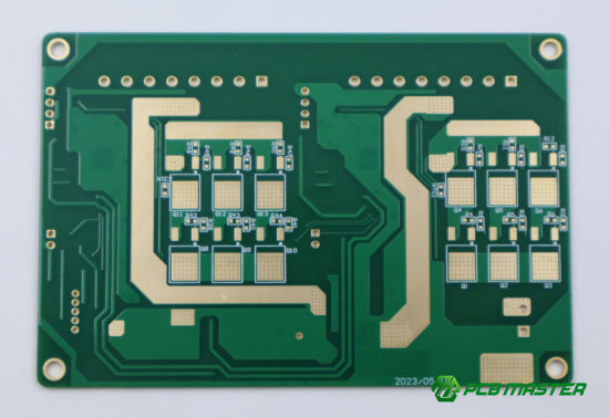
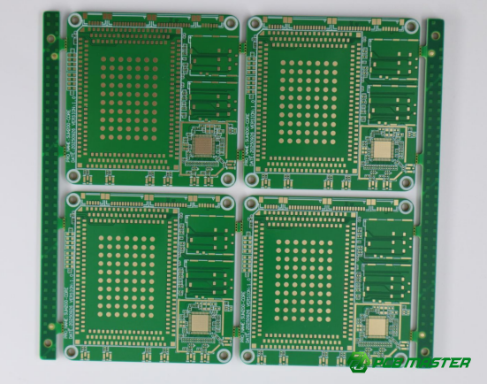
l ENIG is the most widely used method, which involves coating the PCB with a layer of nickel followed by a thin gold layer. This process provides both high solderability and good corrosion resistance. ENIG is ideal for leadless designs like QFN (Quad Flat No-lead) and BGA (Ball Grid Array), where a reliable surface for soldering is crucial.
l Soft Gold is softer and often used in situations where wire bonding is required, such as in high-frequency or high-reliability applications. This gold layer is more pliable and is typically used for more delicate connections.
l Hard Gold, in contrast, is used for high-wear applications. It is more durable and resistant to wear, but it's less commonly used in leadless PCBs.
In leadless PCBs, these gold plating techniques are applied to the pads where the components like QFNs, BGAs, or LGAs (Land Grid Arrays) are attached. These components don't have pins but instead have pads on the PCB’s surface for direct soldering.
How Does Gold Plating Improve Leadless PCB Performance?
Gold plating improves leadless PCB performance by enhancing solderability, minimizing signal loss, maintaining low-resistance electrical contacts, and protecting against oxidation and corrosion, ensuring reliable, long-lasting functionality.
1. Enhancing Solderability and Solder Joint Reliability
Improved Wetting Ability:
Gold plating greatly improves solder adhesion by providing a smooth, uniform surface that helps solder flow more easily. This results in stronger, more reliable solder joints. For leadless components like QFNs and BGAs, which rely on surface-mount soldering, gold-plated pads ensure that the solder bonds effectively and consistently, reducing the likelihood of defects such as cold solder joints or bridges.
For example, in high-speed electronics, where precision soldering is critical, gold plating ensures that each solder joint has a high level of uniformity and reliability, which is crucial for the functionality and longevity of the device.
Benefits in Automated and High-Precision Soldering:
Gold-plated pads are particularly beneficial for automated soldering processes. In modern electronics manufacturing, where machines are used to place and solder components, gold plating ensures that the automated systems can accurately apply solder without causing defects. Gold's smooth surface reduces the chance of issues like misalignment, insufficient solder flow, or solder ball formation, which are common when soldering on rough or oxidized surfaces. This ensures high-quality solder joints in leadless designs, especially for components that require high-precision soldering, such as 5G modules or IoT sensors.
2. Enhancing Electrical Performance
Minimizing Signal Loss and Impedance Mismatch:
Gold plating plays a key role in maintaining the integrity of electrical signals in high-speed and high-frequency designs. The smooth surface of gold ensures that signal degradation is minimized, which is crucial for applications like 5G and high-speed data transmission. Without gold plating, the solder pads could suffer from oxidation or surface irregularities, leading to poor connections and signal loss.
For instance, in 5G communication systems, maintaining a strong signal is essential for performance. Gold-plated pads ensure that the signals travel with minimal interference, keeping the data transfer rates high and stable, even under demanding conditions.
Maintaining Low-Resistance Contacts:
Gold’s excellent electrical conductivity ensures that the connections between components on leadless PCBs are low-resistance, which is essential for ensuring fast, stable electrical performance. High resistance in solder joints or contact pads can cause voltage drops, signal distortion, and energy loss, all of which can degrade the performance of high-speed circuits.
In modern applications like IoT and automotive electronics, where fast response times and high data transfer rates are critical, gold plating ensures that the electrical contacts remain consistently low-resistance, allowing for optimal circuit performance and reducing the risk of signal distortion and data corruption.
3. Preventing Oxidation and Corrosion
Protecting Copper Layers:
One of the biggest challenges in PCB manufacturing is preventing the oxidation of copper pads. Copper, the material typically used in PCBs, is prone to oxidizing when exposed to air and moisture, which can degrade the electrical connections. Gold plating provides a protective barrier over the copper, preventing oxidation and preserving the copper's conductivity over time. This is particularly important in leadless PCBs, where precision and reliability are essential.
In harsh environments like automotive systems or medical devices, where PCBs are exposed to extreme temperatures and humidity, gold plating ensures that the PCB’s performance is not compromised by copper oxidation.
Corrosion Resistance for Long-Term Functionality:
Gold’s corrosion resistance makes it ideal for use in long-life, high-reliability applications. In environments where moisture, heat, or chemicals are present, gold plating acts as a protective shield that prevents the PCB from deteriorating. This ensures the PCB continues to perform reliably over extended periods, even in challenging conditions.
For example, in industrial automation systems, where equipment is exposed to high humidity or fluctuating temperatures, gold-plated PCBs remain functional for longer periods without degradation, making them a preferred choice for mission-critical applications.
How Does Gold Plating Enhance the Reliability of Leadless PCBs?
Gold plating enhances the reliability of leadless PCBs by providing wear resistance, preventing solder joint cracking under mechanical stress, and ensuring stable connections for high-density components in high-performance circuits.
1. Increasing Durability and Longevity
Wear Resistance:
Gold plating provides a durable, wear-resistant surface on leadless PCBs, which helps to prevent mechanical damage and wear, especially in high-usage scenarios. Components on the PCB, such as QFNs and BGAs, are frequently exposed to mechanical stress during handling, assembly, and operation. The gold plating protects the underlying copper and other materials, ensuring the PCB remains functional even with frequent use. For example, in consumer electronics like smartphones or laptops, where parts are used intensively, gold plating ensures that the surface remains intact over time, contributing to the product’s longevity.
Resistance to Thermal Cycling and Environmental Stress:
Gold-plated PCBs also resist thermal cycling and environmental stress better than non-plated boards. The gold coating allows the PCB to expand and contract with temperature changes without affecting its performance. In environments where temperature fluctuations are common, such as in automotive electronics or industrial machinery, gold plating helps the PCB maintain its structural integrity over long periods. This durability ensures that the PCB continues to perform reliably, even under harsh conditions. For instance, in automotive systems, the PCB must endure both high heat under the hood and cold temperatures, which gold plating helps mitigate by preventing cracking and degradation.
2. Gold Plating and Resistance to Mechanical Stress
Preventing Solder Joint Cracking:
Gold’s malleability helps it absorb mechanical stress, reducing the risk of solder joint cracking in leadless PCBs. This is particularly important for devices that are subject to vibration, such as automotive electronics, aerospace applications, and industrial devices. Vibration or physical shock can cause solder joints to crack, leading to potential failures. Gold plating prevents these issues by providing a flexible surface that can withstand mechanical stress without breaking. For example, in automotive control systems, where the PCB is exposed to vibrations and movement, gold plating ensures that the solder joints stay intact, contributing to the overall reliability of the system.
3. Supporting Advanced Components and High-Density Designs
Compatibility with Modern, High-Density Components:
Gold plating is crucial for modern, high-density components that require precise and reliable connections. With the push toward smaller and more powerful electronics, components are becoming more compact and densely packed on the PCB. Gold plating provides the necessary surface for these components to adhere properly and function effectively. In 5G networks, for example, gold-plated pads allow for reliable connections in the high-density circuits that enable fast data transfer. Gold’s ability to maintain integrity under high-density designs ensures that smaller components like capacitors and resistors continue to perform without risk of failure.
Enhancing High-Performance Circuit Reliability:
Gold plating is particularly important for high-performance circuits, which are commonly found in advanced applications such as 5G, IoT, and automotive electronics. These circuits operate at high frequencies and need stable, low-resistance connections to function effectively. Gold's superior electrical conductivity ensures that these circuits remain reliable over time, even under demanding conditions. For example, in 5G technology, gold plating ensures that the high-speed signals pass through the PCB with minimal signal degradation or impedance mismatch, resulting in better performance and reliable data transmission.
Challenges and Considerations in Gold Plating for Leadless PCBs
Cost Considerations
What are the cost implications of gold plating for leadless PCBs?
Gold plating adds extra costs to PCB manufacturing due to the price of gold and the specialized processes required. This can make gold-plated PCBs more expensive than non-plated alternatives, especially in consumer electronics where cost efficiency is critical. However, the additional expense can be justified by the long-term benefits gold plating provides, such as improved reliability, performance, and durability. For example, gold plating’s ability to enhance solderability and reduce signal degradation in high-speed circuits makes it indispensable in high-performance applications like 5G and IoT devices, where reliability is non-negotiable. In lower-cost, high-volume consumer electronics, manufacturers may opt for alternative plating methods like immersion silver or ENIG to balance performance with cost.
Case study example: For mass-market smartphones, the higher cost of gold-plated PCBs might be seen in premium models that require robust, long-lasting performance, while budget models might opt for cheaper plating methods.
Process Complexity and Quality Control
What are the challenges in maintaining uniform plating thickness and quality during gold plating?
Gold plating is a precise process that requires careful control to ensure uniform thickness across the PCB. Variations in the plating thickness can lead to inconsistent soldering, poor electrical performance, or premature wear and tear. Achieving the right balance in plating thickness is particularly important in leadless PCBs (like QFN and BGA) where precise connections are critical. The plating process itself involves several steps—cleaning, coating with nickel, and then applying gold—and any deviations can impact the final product quality.
For example, over-plating might result in excess gold, increasing cost and potentially affecting solderability, while under-plating can lead to weak connections or oxidation. Manufacturers need to closely monitor variables like temperature, time, and solution concentration to ensure high-quality, consistent gold plating.
Case study example: In a factory that produces automotive PCBs, strict quality control is essential to ensure the gold plating remains within specifications to prevent connection failure in high-stress environments, like under the hood of a vehicle.
Environmental Concerns
What sustainable practices can be implemented in gold plating to reduce environmental impact?
Gold plating, like any industrial process, generates waste and environmental concerns. One significant issue is the disposal of chemicals used in the plating process, which can be harmful if not properly managed. To reduce the environmental impact, many manufacturers are adopting sustainable practices, such as recycling gold from waste materials, improving water usage, and using eco-friendly chemicals in the plating bath. Companies can also invest in closed-loop systems where the gold and other chemicals are continuously recycled, reducing both waste and the need for raw materials.
Additionally, gold’s high recyclability makes it a better choice than other metals when it comes to environmental sustainability, as gold can be recovered from electronic waste and reused in new production.
Real-life example: A PCB manufacturer in the automotive industry might use a closed-loop gold recycling system to minimize waste, ensuring that the gold used in high-performance parts, like sensors or control modules, is recycled and reused.
Conclusion
Gold plating plays a crucial role in enhancing both the performance and reliability of leadless PCBs. By improving solderability, electrical performance, and resistance to oxidation, gold plating ensures that these advanced PCBs maintain their functionality under demanding conditions. Whether it's high-frequency applications like 5G or automotive electronics, the durability and superior electrical properties of gold-plated surfaces ensure the PCB continues to perform at its best over time. Moreover, gold plating's ability to withstand thermal cycling and mechanical stress makes it an essential choice for industries requiring long-lasting, high-reliability components.
As the demand for high-performance electronics grows, the importance of gold plating in modern PCBs cannot be overstated. It not only addresses the technical needs of advanced circuits but also ensures the longevity and reliability that are critical in today’s fast-paced technological landscape.
For businesses looking for high-quality PCBs and PCBA solutions, PCBMASTER stands out as a trusted supplier. With years of experience, PCBMASTER is dedicated to delivering top-tier products tailored to meet the specific needs of each customer. Whether it's for consumer electronics, automotive systems, or IoT applications, PCBMASTER ensures that every board is manufactured to the highest standards, supporting the success of modern electronic devices.
FAQs
1. What makes gold plating essential for solderability in leadless PCBs?
Gold plating ensures reliable solder joints by providing a smooth, uniform surface that enhances solder adhesion. This is particularly important for fine-pitch components in leadless designs, such as QFNs and BGAs, where the solder joints must be precisely applied. Gold plating improves wetting ability, allowing the solder to flow evenly and form strong connections without defects. By creating a consistent surface, gold plating helps prevent issues like cold solder joints or bridging, which can occur when the solder does not bond properly to the PCB pad.
2. How does gold plating help reduce signal loss in high-frequency circuits?
Gold plating plays a critical role in minimizing signal loss by providing a low-resistance connection. In high-frequency circuits, like those used in 5G or IoT devices, maintaining signal integrity is crucial for optimal performance. Gold’s superior electrical conductivity ensures that the signals pass through the PCB with minimal resistance or impedance mismatch, which can degrade signal quality. By reducing these losses, gold-plated pads ensure faster data transmission, more stable connections, and improved performance in high-speed applications.
3. Why is gold plating used in PCB designs exposed to harsh environments?
Gold plating is used in harsh environments because of its excellent corrosion resistance. Unlike other metals, gold does not tarnish or oxidize, even when exposed to high humidity or extreme temperatures. This makes it ideal for use in environments where the PCB may face moisture, temperature changes, or exposure to chemicals. Gold’s protective layer ensures that the underlying copper and electrical connections remain intact, extending the lifespan of the PCB and ensuring that it continues to function reliably over time, even in challenging conditions like those found in automotive or medical devices.
4. Can gold plating prevent mechanical failure in leadless PCBs?
Yes, gold plating helps prevent mechanical failure in leadless PCBs by leveraging its malleability. Gold’s flexible nature allows it to absorb mechanical stress, which can occur in vibration-sensitive applications. In devices like automotive electronics or aerospace components, gold plating prevents solder joint cracking by maintaining the structural integrity of the PCB during vibration or thermal expansion. This ensures that the connections remain stable and functional, even under physical stress, leading to reliable performance over the long term.
5. Is gold plating cost-effective for consumer electronics?
Gold plating is generally more expensive than other plating methods due to the high cost of gold and the intricate manufacturing process. However, for high-performance and long-lasting products, the benefits often outweigh the costs. Gold plating enhances solderability, signal integrity, and corrosion resistance, making it a worthwhile investment for premium consumer electronics where durability and reliability are critical. In lower-cost consumer electronics, manufacturers might opt for alternatives like ENIG (Electroless Nickel Immersion Gold) to strike a balance between cost and performance. Ultimately, gold plating is a cost-effective choice for applications where performance, reliability, and long-term durability are prioritized.
Author Bio
Hi, I'm Carol, the Overseas Marketing Manager at PCBMASTER, where I focus on expanding international markets and researching PCB and PCBA solutions. Since 2020, I've been deeply involved in helping our company collaborate with global clients, addressing their technical and production needs in the PCB and PCBA sectors. Over these years, I've gained extensive experience and developed a deeper understanding of industry trends, challenges, and technological innovations.
Outside of work, I'm passionate about writing and enjoy sharing industry insights, market developments, and practical tips through my blog. I hope my posts can help you better understand the PCB and PCBA industries and maybe even offer some valuable takeaways. Of course, if you have any thoughts or questions, feel free to leave a comment below—I'd love to hear from you and discuss further!

