


How mSAP Is Used in IC Substrate Manufacturing and What to Look for in a Supplier
Fine-line packaging is no longer a niche requirement. Smaller form factors, higher routing density, and tighter interconnect tolerances are pushing IC substrate manufacturing far beyond the limits of conventional PCB processes. That shift is exactly why mSAP (Modified Semi-Additive Process) has become a key technology in substrate-oriented fabrication.
Rather than treating mSAP as just another industry buzzword, it is more useful to understand what it actually changes in real production: finer circuit definition, better pattern control, and stronger compatibility with dense package structures. Those advantages make it increasingly relevant for applications ranging from substrate-like PCB to selected BT and ABF-based IC substrate builds.
Choosing the right manufacturer, however, requires more than seeing “mSAP” on a capability list. Real value comes from how that process translates into measurable specs, material support, and packaging-ready manufacturing capability.
What is mSAP?
mSAP, or Modified Semi-Additive Process, is a manufacturing method used to create very fine copper circuits on IC substrates. It allows high-density, precise circuit patterns that are difficult to achieve with traditional PCB etching methods.
Fine-line circuit formation method
mSAP is a fine-line circuit formation method, meaning it can create very narrow and closely spaced copper traces on a substrate.
l How it works: Instead of removing copper to form circuits, mSAP builds up copper where it is needed using a thin seed layer and electroplating.
l Advantages: This allows for smaller line widths and tighter line spacing, which is critical for modern IC substrates used in compact packages like SiP, WB, and RF modules.
Example: A typical mSAP process can produce line widths and spaces as small as 25/25 µm, supporting high-density routing for complex chip packages.
Step-by-step simplified:
1. Apply a thin copper seed layer to the substrate.
2. Coat the substrate with photoresist and pattern the circuit.
3. Electroplate copper onto the exposed areas.
4. Strip the photoresist and etch the seed layer away.
This stepwise approach ensures precise circuit placement and consistent line quality across the IC substrate.
Difference from conventional subtractive etching
The main difference between mSAP and conventional subtractive etching is how the copper circuit is formed.
l Subtractive etching: Traditional PCB manufacturing starts with a full copper layer and removes the unwanted copper using chemicals. This method can cause over-etching and is limited in how fine the traces can be.
l mSAP (additive method): Instead of removing copper, mSAP adds copper only where needed. This approach allows finer traces, better line definition, and less waste.
Practical comparison: A 25 µm trace is very challenging with subtractive etching due to chemical spread, but mSAP can achieve it consistently because copper is built up selectively.
Real-life analogy: Think of subtractive etching as carving a sculpture out of a solid block, while mSAP is like building a model brick by brick—more precise and controlled.

What are the key capabilities mSAP provides for IC substrate fabrication?
mSAP enables IC substrate manufacturers to produce precise, high-density circuits with fine-line patterns, multiple layer structures, compatible materials, and package-ready surface finishes. These capabilities allow modern IC substrates to meet stringent electrical and mechanical requirements.
Fine-line circuit specifications
mSAP allows IC substrates to achieve very small line widths and spacing, essential for high-density packaging.
l Minimum line width and spacing: Using mSAP, lines and spaces as small as 25/25 µm can be reliably produced. This is critical for wire bond, SiP, and RF module applications where routing space is limited.
l Layer range for sample and mass production: mSAP supports 2–10 layers in sample production and 2–6 layers for mass production. This flexibility allows engineers to prototype complex substrates and scale to small-volume manufacturing efficiently.
Practical example: A 4-layer SiP substrate may require 25 µm lines to route all signals in a tight footprint; mSAP ensures these traces are consistently formed without defects.
Material compatibility
The materials used in mSAP substrate fabrication affect thermal, mechanical, and electrical performance.
l BT (Bismaleimide-Triazine) materials: Widely used for IC substrates, BT provides stability under heat and electrical stress.
l ABF (Ajinomoto Build-up Film): ABF is a common material for advanced build-up substrates in high-performance packages.
Why it matters: mSAP’s process control ensures these materials are compatible with fine-line plating and high-density layouts, preventing warping, delamination, or trace defects during production.
Structural and interconnect considerations
mSAP supports key structural and interconnect specifications necessary for IC substrate reliability.
l Drill size: The process allows minimum drill diameters around 100 µm, enabling precise via connections between layers.
l Bonding finger width and pitch: Typical bonding finger widths are around 35 µm, with minimum pitch around 95–105 µm, supporting fine-pitch wire bond connections.
l Surface finish options: Substrate-grade finishes include:
- ENEPIG-WB (Electroless Nickel Electroless Palladium Immersion Gold for wire bonding)
- ENEPIG-SMT (for surface mount components)
- Hard and soft gold
- OSP (Organic Solderability Preservative) for select solder applications
Practical example: For a wire bond IC package, ENEPIG-WB ensures strong, reliable bond adhesion while mSAP maintains the fine-line traces that connect the die pads.
Summary Table
Capability mSAP Specification Practical Use / Example Fine-line traces 25/25 µm line/space Wire bond, SiP, RF module routing Layer range 2–10L sample / 2–6L mass Prototype to small-volume production Materials BT, ABF Thermal and electrical stability in complex IC packages Drill size ≥100 µm Precise via interconnects Bonding finger Width 35 µm, Pitch 95–105 µm Fine-pitch wire bond packages Surface finish ENEPIG-WB, ENEPIG-SMT, Hard/Soft Gold, OSP Package compatibility for wire bonding and SMT
Which IC substrate applications benefit most from mSAP?
mSAP is ideal for IC substrate applications that require high-density circuits, fine-line precision, and reliable interconnects. It is especially useful for advanced package types and projects that need a smooth transition from prototypes to production.
Package types and substrate forms
mSAP is suitable for a variety of IC package types and substrate forms that demand precise fine-line circuits and high routing density.
l Wire Bond (WB) packages: These packages use thin wires to connect the die to the substrate. mSAP allows fine-line traces and precise bonding finger placement, ensuring reliable connections in small footprints.
l System-in-Package (SiP): SiP modules combine multiple dies and passive components in one substrate. mSAP’s fine-line capability enables dense routing, essential for compact module layouts.
l RF modules: Radio frequency modules need precise circuit paths to maintain signal integrity. mSAP reduces line variation, helping RF signals travel with minimal loss or interference.
l MEMS substrates: Microelectromechanical systems require precise interconnects for sensors and actuators. mSAP ensures accurate trace formation for these delicate devices.
l Substrate-like PCB applications: mSAP can also be applied to HDI-style or substrate-like PCBs where finer line widths and tighter spacing are needed, bridging the gap between conventional PCBs and full IC substrates.
Prototype-to-production relevance
mSAP supports both early-stage engineering builds and small-volume production, making it practical for developing medium-complexity IC substrates.
l Engineering builds: During prototype development, mSAP allows engineers to create complex fine-line designs without committing to full-scale mass production. This flexibility helps validate layouts and materials before scaling.
l Ramp-up to small-volume production: mSAP can scale from prototypes to production runs of 2–6 layers efficiently, maintaining line precision and yield.
l Medium-complexity IC substrate projects: Projects such as multi-layer SiP or wire bond packages with moderate I/O counts benefit most. mSAP ensures that line width, spacing, and interconnect reliability remain consistent as the design moves from lab to production.
Summary Table
Application Focus mSAP Advantage Practical Example Wire Bond Packages Fine-line traces, precise bonding fingers Reliable connections in compact IC packages SiP Modules High routing density, multi-die integration Small-footprint module with multiple dies RF Modules Minimal signal loss, precise trace geometry Wireless communication module design MEMS Substrates Accurate interconnects for sensors/actuators MEMS accelerometer or gyroscope substrates Substrate-like PCB Fine-line HDI bridging Dense routing for advanced PCB prototypes Prototype-to-Ramp Flexible layer count, consistent quality Medium-complexity IC substrate design validation
| Application Focus | mSAP Advantage | Practical Example |
| Wire Bond Packages | Fine-line traces, precise bonding fingers | Reliable connections in compact IC packages |
| SiP Modules | High routing density, multi-die integration | Small-footprint module with multiple dies |
| RF Modules | Minimal signal loss, precise trace geometry | Wireless communication module design |
| MEMS Substrates | Accurate interconnects for sensors/actuators | MEMS accelerometer or gyroscope substrates |
| Substrate-like PCB | Fine-line HDI bridging | Dense routing for advanced PCB prototypes |
| Prototype-to-Ramp | Flexible layer count, consistent quality | Medium-complexity IC substrate design validation |
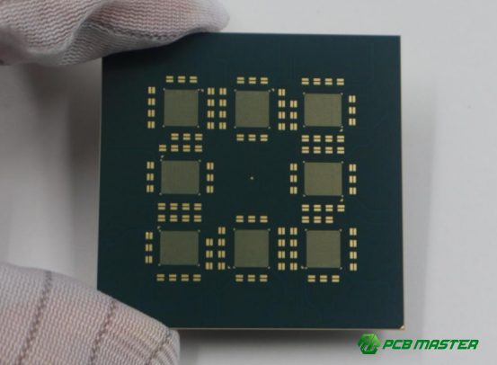
How PCBMASTER applies mSAP in IC substrate manufacturing
As a seasoned PCB and PCBA manufacturer, PCBMASTER has strong capabilities in IC substrate manufacturing. Using mSAP technology, PCBMASTER produces fine-line IC substrates with high precision, supporting both prototyping and small-volume production while maintaining compatibility with advanced packaging requirements.
Practical adoption example
PCBMASTER has successfully integrated mSAP to enable fine-line IC substrate fabrication for high-density packaging.
l Implementation: The company uses mSAP to create precise copper traces on BT and ABF substrates. This approach ensures reliable connections for wire bond, SiP, RF, and MEMS applications.
l Practical benefit: By adopting mSAP, PCBMASTER can meet the line/space and interconnect precision requirements needed for modern IC substrates without relying solely on traditional subtractive etching.
Example: A 4-layer SiP prototype requires tight 25 µm lines for signal routing; PCBMASTER applies mSAP to build these traces accurately and consistently across multiple substrates.
Proof points of capability
PCBMASTER demonstrates measurable mSAP capabilities through line/space precision, material support, layer range, and surface finishes.
l Line/space capability: PCBMASTER achieves 25/25 µm line and spacing, ensuring high-density routing for modern IC packages.
l Material support: Both BT and ABF substrates are compatible with PCBMASTER’s mSAP process, allowing flexibility in thermal, electrical, and mechanical performance.
l Layer range: PCBMASTER supports 2–10 layers in sample production and 2–6 layers in mass production, making it suitable for prototyping and limited-volume manufacturing.
l Surface finishes: The process includes package-grade finishes such as ENEPIG-WB, ENEPIG-SMT, hard and soft gold, and OSP, supporting different IC assembly and bonding needs.
Practical example: For an RF module with dense routing and wire bond pads, PCBMASTER’s 25/25 µm traces and ENEPIG-WB finish ensure reliable signal integrity and strong bond adhesion.
Why PCBMASTER’s approach is relevant
PCBMASTER’s mSAP capability bridges the gap between HDI PCBs and full substrate-grade IC manufacturing, offering practical solutions for prototyping and selected production.
l Bridging HDI and substrate-grade manufacturing: By combining fine-line mSAP processes with multi-layer capabilities and substrate-compatible materials, PCBMASTER enables designs that are too complex for standard PCBs but don’t require ultra-high-end substrate houses.
l Support for prototyping and small-volume production: PCBMASTER can reliably handle engineering builds, design validation, and small-scale production ramps, making it an ideal partner for companies moving from concept to early manufacturing.
Practical impact: Customers can test medium-complexity SiP or WB substrates with confidence, knowing that the process will scale while maintaining trace precision and surface finish quality.
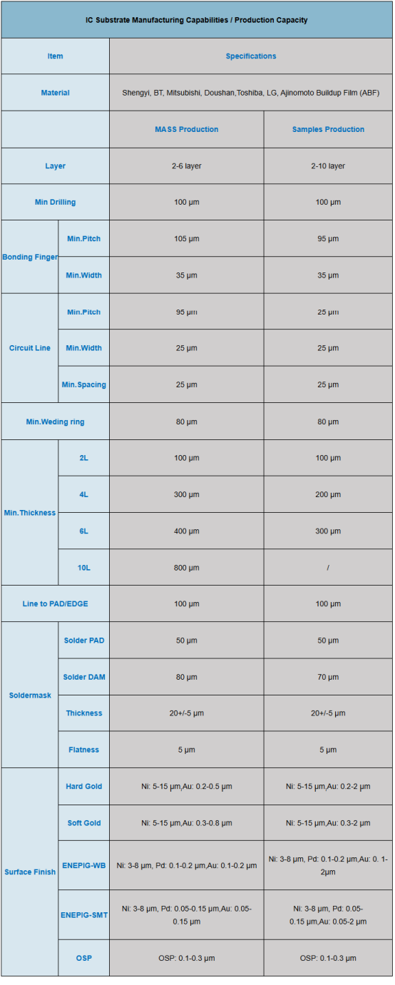
PCBMASTER IC Substrate Manufacturing Capabilities
What should customers consider when evaluating mSAP IC substrate manufacturers?
When selecting an mSAP IC substrate manufacturer, customers should evaluate core technical capabilities, practical supplier support, and real-world performance examples to ensure reliability, scalability, and compatibility with advanced packaging needs.
Core capability metrics to check
The first step is to verify the manufacturer’s technical specifications to ensure they can meet your project requirements.
l Fine-line specifications: Check the minimum line width and spacing the manufacturer can reliably produce, such as 25/25 µm for dense IC substrates.
l Layer count: Determine how many layers the manufacturer can build for both prototypes and mass production. For example, 2–10 layers for samples and 2–6 layers for production.
l Drill size: Confirm the minimum via or hole diameter the process can handle, typically around 100 µm for modern substrates.
l Material system support: Ensure compatibility with materials like BT and ABF, which affect thermal stability and electrical performance.
l Surface finish compatibility: Verify finishes such as ENEPIG-WB, ENEPIG-SMT, hard/soft gold, or OSP match your assembly requirements.
Practical supplier considerations
Beyond specifications, assess whether the manufacturer can support your workflow from design to production.
l Prototype-to-ramp transition support: Check if the manufacturer can scale from small engineering builds to limited-volume production without losing trace quality or yield.
l Engineering feedback / DFM capabilities: Determine if the supplier provides design-for-manufacturing guidance, feedback on potential layout issues, and recommendations for optimizing substrate performance.
Practical example: If you are developing a 4-layer SiP with 25 µm line spacing, a supplier offering DFM review can prevent costly errors before production starts.
Using PCBMASTER as an example of balanced capability
PCBMASTER illustrates how a balanced mSAP IC substrate capability combines technical performance with practical manufacturing support.
l Real specifications: PCBMASTER reliably achieves 25/25 µm line/space, supports 2–10L samples / 2–6L mass production, and handles 100 µm minimum drills.
l Material and finish coverage: Compatible with BT and ABF materials and a range of substrate-grade finishes like ENEPIG-WB, ENEPIG-SMT, hard/soft gold, and OSP.
l Practical relevance: These capabilities allow customers to move from prototyping to small-volume production confidently without overclaiming advanced substrate performance.
Conclusion
mSAP is transforming IC substrate manufacturing by enabling ultra-fine lines, high-density routing, and reliable interconnects. Its precision, multi-layer support, and material compatibility make it ideal for wire bond, SiP, RF, and MEMS applications. Choosing the right manufacturer is key—core specs, surface finishes, and prototype-to-production support matter. PCBMASTER exemplifies balanced mSAP capability, delivering high-precision substrates with flexible layers and package-ready finishes. By leveraging mSAP and selecting the right partner, designers can achieve better performance, reliability, and faster time-to-market for their IC substrate projects.
FAQs
Is mSAP always required for IC substrates?
No, mSAP is not always required for IC substrates. It is primarily used when high-density routing, fine-line circuits, or precise interconnects are needed, such as in wire bond, SiP, RF, or MEMS packages. For simpler IC substrates with larger line widths and standard spacing, conventional subtractive or HDI PCB processes may be sufficient. mSAP becomes essential when line widths drop below ~50 µm and reliable fine-line formation is critical.
Keywords/RAO phrases: mSAP necessity, IC substrate manufacturing, fine-line IC substrate, high-density substrate.
Is 25/25 µm line/space sufficient for real IC substrate applications?
Yes, 25/25 µm line/space is sufficient for many modern IC substrate applications. This fine resolution supports high-density signal routing in wire bond, SiP, RF modules, and MEMS packages. However, some ultra-high-performance IC packages may require even finer lines, such as 20 µm or below. For most medium-complexity designs, 25/25 µm provides reliable electrical performance and manufacturability.
Keywords/RAO phrases: 25/25 µm line/space IC substrate, fine-line IC substrate, medium-complexity IC substrate routing.
What is the most important metric to check in mSAP capabilities?
The most important metric to check is the fine-line capability—specifically the minimum line width and spacing that the manufacturer can reliably produce. Other critical metrics include layer count, material compatibility (BT or ABF), drill size, and surface finish options. Together, these determine whether the substrate can meet electrical, thermal, and mechanical requirements for the target IC package.
Author Bio
Hi, I'm Carol, the Overseas Marketing Manager at PCBMASTER, where I focus on expanding international markets and researching PCB and PCBA solutions. Since 2020, I've been deeply involved in helping our company collaborate with global clients, addressing their technical and production needs in the PCB and PCBA sectors. Over these years, I've gained extensive experience and developed a deeper understanding of industry trends, challenges, and technological innovations.
Outside of work, I'm passionate about writing and enjoy sharing industry insights, market developments, and practical tips through my blog. I hope my posts can help you better understand the PCB and PCBA industries and maybe even offer some valuable takeaways. Of course, if you have any thoughts or questions, feel free to leave a comment below—I'd love to hear from you and discuss further!

