


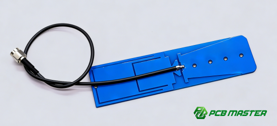
PCB Antenna with or without Solder Mask: Design and Manufacturing Tradeoffs
When designing a PCB antenna, one often overlooked but highly impactful decision is whether the antenna area should be covered with solder mask or left exposed (no solder mask opening).
This choice directly affects:
l Resonant frequency
l Bandwidth
l Radiation efficiency
l Impedance matching
l Environmental stability
l Long-term reliability
l Manufacturing difficulty
l Yield and cost
In short, “cover” vs “no cover” is not just a cosmetic PCB choice—it is a system-level RF decision.
For most products, the right answer depends on one core tradeoff:
l Cover with solder mask if you want better protection, higher production consistency, and easier mass manufacturing
l Leave the antenna exposed if you need maximum RF performance, especially at higher frequencies, and you can tightly control structure, process, and testing
This article explains how to make that decision clearly from both the design side and the manufacturing side.
What Is the Difference Between a PCB Antenna with Solder Mask and Without Solder Mask?
What “covered with solder mask” means
A covered PCB antenna means the copper antenna trace is coated by the PCB’s solder mask layer.
In this case:
l The antenna sits under an additional dielectric layer
l The local RF environment is more stable
l The copper is protected from oxidation and mechanical damage
The antenna no longer “sees” only air above it
What “no solder mask” means
A PCB antenna without solder mask means the antenna region is opened in the solder mask, leaving the copper surface or its surface finish exposed.
In this case:
l The antenna is closer to an air dielectric environment
l There is no added solder mask dielectric loss
l RF performance may improve
l But the antenna becomes more sensitive to external materials, contamination, handling, and aging
Why this matters in RF design
Solder mask is not electrically invisible.
It introduces:
l Dielectric loading
l Loss tangent
l Impedance shift
l Frequency detuning
l Environmental stabilization
That is why the same antenna geometry can behave differently depending on whether it is covered or exposed.
Does Solder Mask Change PCB Antenna Frequency, Bandwidth, and Impedance?
Yes—solder mask can shift antenna frequency downward
A solder mask layer has a dielectric constant typically around εr ≈ 3.2–4.5 (depending on material and vendor).
When this layer covers the antenna:
l The effective dielectric constant seen by the antenna increases
l The electrical length becomes longer
l The resonant frequency shifts lower
This is one of the most common reasons why:
l Simulation looks correct
l Prototype appears acceptable
l But mass production shifts the antenna band downward
How much frequency shift should you expect?
There is no universal fixed number.
The shift depends on:
l Antenna type (IFA, PIFA, meandered trace, patch, etc.)
l Frequency band
l Antenna dimensions
l Solder mask thickness
l Solder mask dielectric constant
l Distance to nearby ground and components
In compact 2.4 GHz and 5 GHz designs, even a small dielectric change can be significant.
Why solder mask can also affect bandwidth
Solder mask does not only move the center frequency.
It can also affect:
l The antenna Q factor
l The shape of the S11 curve
l The usable bandwidth margin
This becomes more important in:
l Narrow-band sub-GHz designs
l Tight 2.4 GHz designs with little margin
l 5 GHz and higher-frequency designs where tolerance windows are smaller
Solder mask also changes transmission line impedance
If your PCB antenna uses:
l A microstrip feed
l Matching stub
l Controlled impedance trace
Then covering those RF traces with solder mask can reduce characteristic impedance.
For example:
l A line designed as 50 ohms without mask
l May become 45–48 ohms after mask coverage (depending on stack-up and geometry)
This can cause:
l Feed mismatch
l Reduced power transfer
l Lower efficiency
l Worse return loss
Design rule: model the solder mask explicitly
If the antenna will be covered in production, the solder mask must be included in:
l EM simulation
l Impedance calculation
l Feedline design
l Matching network tuning
Typical compensation methods include:
l Slightly reducing antenna length
l Adjusting trace width
l Re-tuning matching components
l Rechecking the feedline, not just the radiator
Key principle: If production uses solder mask, simulation must use solder mask.
Does a PCB Antenna Without Solder Mask Always Deliver Higher Efficiency?
In theory, yes—because one loss source is removed
A PCB antenna without solder mask removes:
l The extra dielectric layer
l The dielectric loss associated with that layer
That means the antenna can achieve:
l Slightly higher radiation efficiency
l Lower RF loss
l Better high-frequency performance potential
This is especially valuable when:
l RF margin is tight
l Transmit power budget matters
l Receiver sensitivity matters
l The product operates at 5 GHz or above
The benefit is much more visible at higher frequencies
At lower frequencies (for example, below 1 GHz):
l Solder mask loss is often small
l The practical benefit of opening the antenna may be limited
At 2.4 GHz:
l The difference may be noticeable, depending on antenna size and mask material
At 5 GHz or millimeter-wave:
l Solder mask loss and dielectric sensitivity become much more important
l Exposed antenna regions may offer more meaningful gains
But “higher theoretical efficiency” does not always mean “better final product”
This is where many teams make the wrong assumption.
A no-mask antenna may have:
l Better lab efficiency in isolation
l But worse performance in the real product
Why?
Because an exposed antenna is more sensitive to:
l Plastic housing thickness
l Nearby foam or adhesive
l User hand effects
l Assembly tolerances
l Nearby metal objects
l Gap changes between PCB and enclosure
So while bare-board efficiency may improve, the assembled product may become less stable and may even perform worse overall.
Important: Final antenna decisions should be based on assembled product OTA results, not only bare PCB S11.
Which Option Is More Stable in Real Product Environments?
A solder-mask-covered antenna is usually more stable in mass production
When solder mask covers the antenna:
l The top dielectric environment is more fixed
l The antenna is less directly exposed to surrounding material variation
l Sensitivity to minor assembly changes is often lower
This usually helps with:
l Production consistency
l Unit-to-unit repeatability
l Multi-vendor PCB consistency
l Easier RF control in high-volume manufacturing
An exposed antenna is more sensitive to nearby materials
A no-mask antenna “sees” more of the real world.
That means performance can change more with:
l Enclosure material
l Enclosure wall thickness
l Air gap
l Glue
l Foam pads
l Label films
l Battery position
l Shield can distance
l Screws and metal brackets
l User hand proximity
This is especially important in:
l Handheld products
l Wearables
l Compact IoT devices
l Tight industrial housings
l Products with late mechanical changes
What must be tested during product validation
If you use a no-mask antenna, you should validate at minimum:
l Bare board vs. assembled unit
l Different enclosure material lots
l Different enclosure thickness conditions
l Hand grip or body proximity conditions
l Variations in screw torque / assembly gap
l Battery / shield can positional tolerance
l Adhesive / foam placement impact
For either option, but especially for no-mask designs, you should verify:
l S11 / VSWR
l Resonant frequency shift
l Bandwidth coverage
l OTA efficiency
What Are the Reliability Risks of a PCB Antenna Without Solder Mask?
Exposed copper is more vulnerable over product lifetime
Even with surface finish, an exposed antenna region can face long-term risks such as:
l Oxidation
l Moisture exposure
l Surface contamination
l Corrosion in harsh environments
l Cosmetic or mechanical wear during handling
These issues may not cause immediate failure, but they can cause:
l Gradual RF drift
l Increased loss
l Reduced repeatability
l Reliability concerns over time
Solder mask provides strong environmental protection
A covered antenna benefits from:
l Anti-oxidation protection
l Moisture resistance
l Corrosion resistance
l Better resistance in high humidity
l Better resistance in salt or contaminated environments
This makes solder mask coverage more suitable for:
l Automotive electronics
l Outdoor devices
l Industrial equipment
l Long-life products
l Products with harsh environmental exposure
Mechanical damage risk is much higher without solder mask
A no-mask antenna is more vulnerable during:
l PCB handling
l Depaneling
l Storage
l SMT line transfer
l Manual assembly
l Functional test
l Rework
Common risks include:
l Scratches
l Finger contamination
l Metal debris attachment
l Surface finish damage
l Accidental contact by tools or fixtures
Electrical shorting and insulation risk are often underestimated
Without solder mask, the antenna region is more exposed to accidental contact from:
l Shield cans
l Screws
l Metal brackets
l Conductive foam
l Test fixtures
l Loose solder balls or debris
If the mechanical design does not guarantee sufficient air clearance, the risk increases sharply.
This is one reason many teams choose solder mask coverage even when RF performance could be slightly better without it.
How Do Manufacturing Cost, Process Complexity, and Yield Compare?
Covered antennas fit standard PCB process flow
A solder-mask-covered antenna typically aligns with normal PCB manufacturing:
l Standard process
l Lower handling risk
l Better consistency
l Easier inspection criteria
l Fewer special instructions to the board house
This usually means:
l Lower cost
l Better yield
l Easier scaling
l Less supplier management effort
No-mask antennas increase process control burden
An exposed antenna region often requires stricter control in:
l Solder mask opening definition
l Surface finish quality
l Cleanliness
l Packaging
l Storage conditions
l Transport protection
l Post-fabrication aging control
In some cases, teams may also specify special surface finish considerations to reduce oxidation risk.
Common yield risks for exposed antenna regions
Typical no-mask defect risks include:
l Copper scratches
l Surface contamination
l Solder mask opening burrs
l Uneven edge quality
l Oxidation after storage
l Handling marks
l Surface finish inconsistency
These issues can create:
l Cosmetic rejects
l RF drift
l Field reliability concerns
l Hard-to-troubleshoot performance variation
Factory-side controls become more important
If the antenna is left exposed, manufacturing should tighten control on:
l Opening size tolerance
l Opening alignment
l Surface finish consistency
l Visual inspection criteria
l Clean packaging
l Anti-scratch packaging
l Moisture control
l Storage time limits
l Handling instructions at assembly sites
Bottom line: No-mask designs can work well, but they require stronger process discipline.
How Should Engineers Decide Whether to Cover a PCB Antenna with Solder Mask?
Start with the frequency band
A practical first filter:
l Sub-1 GHz: prioritize stability and reliability unless performance margin is very tight
l 2.4 GHz: balance efficiency vs mass-production consistency
l 5 GHz and above: evaluate no-mask more seriously because loss and detuning sensitivity are higher
Then define the real product priority
Ask this first:
l Is this product performance-first?
l Or mass-production-first?
If your priority is:
l High yield
l Stable tuning
l Lower cost
l High reliability
l Fewer RF surprises during scale-up
Then covered with solder mask is often the safer default.
If your priority is:
l Maximum efficiency
l Higher-frequency optimization
l Aggressive RF performance targets
l Very limited antenna area
l High-end wireless performance
Then no solder mask may be worth evaluating.
Check whether the mechanical design can support a no-mask antenna
Before approving an exposed antenna, verify:
l Adequate air clearance around the antenna
l No nearby metal hardware
l Stable enclosure spacing
l Controlled plastic thickness
l Limited user-hand detuning risk
l Low likelihood of future mechanical changes
If these conditions are weak, no-mask becomes much riskier.
Make sure the team has enough validation capability
A no-mask antenna should not be chosen if the project lacks:
l Multiple prototype iterations
l EM simulation with realistic structure
l OTA validation
l Mechanical variation testing
l Environmental testing
l Supplier consistency checks
If validation bandwidth is limited, solder mask coverage is usually the better production decision.
What Should Design, Manufacturing, and Test Teams Control?
Design team checklist
The design team should define early whether the antenna is:
l Covered by solder mask
l Or opened with no mask
Then they should lock:
l EM simulation assumptions
l Solder mask dielectric model
l Feedline impedance targets
l Antenna geometry compensation
l Matching network tuning strategy
l Keep-out region rules
l Mechanical clearance requirements
Do not change this decision late in the project.
A last-minute switch from “covered” to “no cover” (or vice versa) can invalidate RF tuning.
Manufacturing team checklist
The PCB and assembly teams should control:
l Solder mask opening dimensions
l Opening registration tolerance
l Edge quality around opening
l Surface finish type and consistency
l Copper surface cleanliness
l Packaging and anti-scratch protection
l Moisture and storage conditions
l Handling restrictions during assembly and test
Test team checklist
The RF validation team should verify:
l S11 / return loss
l VSWR
l Resonant frequency
l Bandwidth margin
l Efficiency
l TRP / TIS (if relevant)
l Unit-to-unit consistency
l Performance before and after environmental stress
For exposed antennas, it is strongly recommended to compare:
l Initial performance
l Aged performance
l Humidity exposure
l Repeated handling impact
Common Mistakes When Choosing Solder Mask Coverage for PCB Antennas
Mistake 1: Assuming no solder mask is always better
No-mask is not automatically better.
It may improve theoretical efficiency, but it can also create:
l More detuning
l More variation
l More reliability risk
l Lower mass-production confidence
Mistake 2: Adjusting only the antenna shape but ignoring the feedline
If solder mask changes:
l The antenna resonator
l The microstrip feed
l The matching stub
Then tuning only the radiator is incomplete.
You must also review:
l Feed width
l Controlled impedance
l Matching network values
Mistake 3: Judging only by bare-board measurements
Bare board S11 is useful, but not sufficient.
Real product behavior depends on:
l Housing
l Assembly
l Human interaction
l Nearby metal
l Production tolerances
Always validate in the final product state.
Mistake 4: Treating solder mask removal as a late-stage “fix”
In some emergency cases, engineers may:
l Scrape mask
l Add local dielectric
l Use tape or glue for temporary tuning experiments
These are useful for debug, but they are not robust mass-production strategies.
If no-mask is the right production choice, it should be designed intentionally from the beginning.
Practical Recommendation: When Should You Cover the PCB Antenna, and When Should You Leave It Exposed?
Choose a solder-mask-covered antenna when:
l Production consistency matters most
l Reliability requirements are high
l The product has a long service life
l The environment includes humidity, corrosion, or outdoor exposure
l Mechanical tolerances are not tightly controlled
l The antenna is close to other structures
l The project has limited RF iteration cycles
l Cost and yield are important
This is the default choice for many commercial products.
Consider a no-solder-mask antenna when:
l You need the highest possible RF efficiency
l The design operates at 5 GHz or higher
l The antenna area is very limited
l RF margin is tight
l The product can tolerate higher process control burden
l Mechanical spacing is well controlled
l You have strong RF validation resources
l The product is performance-driven rather than cost-driven
This is a more advanced choice and should be validated carefully.
Best real-world decision rule
A practical engineering rule is:
If there is no strong RF reason to open the antenna area, keep it covered with solder mask.
Only choose no-mask when there is a clear performance benefit and the team can manage the added manufacturing and reliability risks.
Quick Comparison Table: PCB Antenna with vs. without Solder Mask
| Item | Covered with Solder Mask | No Solder Mask (Exposed) |
| Resonant Frequency | Usually shifts lower unless compensated | Closer to air-loaded expectation |
| Bandwidth Control | Requires dielectric-aware tuning | More direct, but more environment-sensitive |
| Radiation Efficiency | Slightly lower due to dielectric loss | Potentially higher |
| High-Frequency Performance | More loss at 5 GHz / mmWave | Better potential performance |
| Impedance Control | Feedline impedance changes under mask | Easier baseline modeling, but surface finish matters |
| Environmental Stability | Better | Worse |
| Mechanical Protection | Better | Worse |
| Oxidation / Corrosion Risk | Lower | Higher |
| Shorting / Contact Risk | Lower | Higher |
| Manufacturing Complexity | Lower | Higher |
| Production Yield | Higher | More sensitive |
| Cost | Lower / standard | Often higher |
| Best For | Stable mass production | RF-optimized high-performance designs |
Conclusion
Choosing whether to cover a PCB antenna with solder mask is a practical RF engineering decision with direct consequences for:
l Frequency accuracy
l Bandwidth margin
l Impedance matching
l Radiation efficiency
l Environmental stability
l Reliability
l Manufacturing complexity
l Yield and cost
The simplest and most useful conclusion is this:
l Use solder mask coverage when you want a safer, more robust, and more manufacturable design
l Use no solder mask only when there is a clear RF performance advantage and your team can control the added process, structural, and reliability risks
For most production programs:
l If there is no strong RF reason to remove solder mask, keep the antenna covered.
l If performance demands justify exposure, validate the decision at the assembled product level—not just on the bare PCB.
That is the difference between a lab-tuned antenna and a production-ready antenna.
If you have any further questions or would like more information, feel free to contact PCBMASTER. As an experienced PCB and PCBA supplier, we not only provide high-quality products, but are also happy to offer professional answers and practical engineering support for your project.
FAQs
1. Does a 2.4 GHz PCB antenna always need a solder mask opening?
No. A 2.4 GHz PCB antenna does not always need to be exposed. Many 2.4 GHz products perform well with solder mask coverage, especially when consistency, yield, and environmental stability matter more than chasing the last bit of efficiency.
2. How much does solder mask shift PCB antenna frequency?
There is no universal number. The shift depends on:
l Antenna type
l Frequency band
l Solder mask thickness
l Dielectric constant
l Geometry and nearby structures
The correct approach is to include solder mask in simulation and verify with prototype measurement.
3. Is no solder mask better for 5 GHz PCB antennas?
Often, it is more worth evaluating at 5 GHz because dielectric loss and detuning sensitivity are more significant. However, it is not automatically better in the final product unless enclosure and process variation are tightly controlled.
4. What surface finish should be used if the antenna is exposed?
The best surface finish depends on:
l Frequency band
l Oxidation risk
l Product lifetime
l Cost target
l Factory capability
The key is not just the finish itself, but consistency, aging behavior, and RF validation after exposure conditions.
5. Can I scrape solder mask off a tuned antenna to fix frequency?
You can use this as a debug experiment, but it should not be treated as a formal production solution. If removing solder mask improves performance, the antenna should be redesigned and revalidated intentionally rather than relying on manual rework.
Author Bio
Hi, I'm Carol, the Overseas Marketing Manager at PCBMASTER, where I focus on expanding international markets and researching PCB and PCBA solutions. Since 2020, I've been deeply involved in helping our company collaborate with global clients, addressing their technical and production needs in the PCB and PCBA sectors. Over these years, I've gained extensive experience and developed a deeper understanding of industry trends, challenges, and technological innovations.
Outside of work, I'm passionate about writing and enjoy sharing industry insights, market developments, and practical tips through my blog. I hope my posts can help you better understand the PCB and PCBA industries and maybe even offer some valuable takeaways. Of course, if you have any thoughts or questions, feel free to leave a comment below—I'd love to hear from you and discuss further!

