


Why Use PCB Edge Plating? Benefits, Applications, and Design Tips
PCB edge plating is often treated as a niche PCB process, but in many designs, it solves very practical engineering problems. When a board edge must do more than define the outline—such as improve grounding continuity, support EMI control, strengthen mechanical reliability, or enable edge-side electrical contact—standard edge clearance is no longer enough.
That is why edge plating appears in high-reliability, high-frequency, and structure-sensitive PCB applications. It is not a decorative upgrade or a default fabrication option. It is a functional design choice that should be evaluated only when the board edge needs to serve a clear electrical or structural purpose.
This article focuses on a simple question: why design PCB edge plating? Rather than treating it as a generic “special process,” the discussion will look at when it adds real value, where it is most useful, what limitations it introduces, and how to judge whether it is truly worth specifying in a PCB design.
What Is PCB Edge Plating, and Why Is It Not the Same as Ordinary Exposed Copper at the Board Edge?
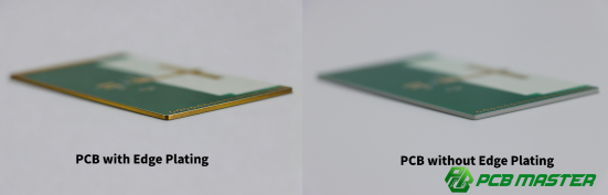
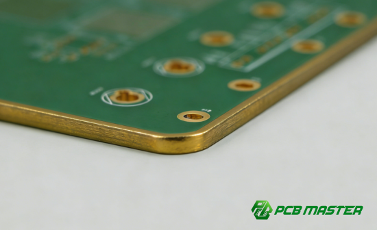
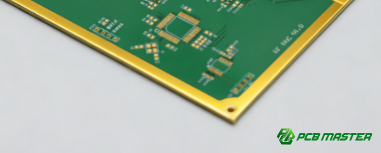
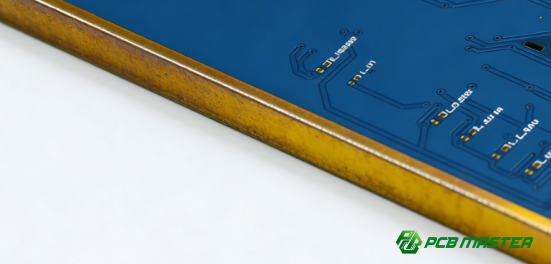
PCB edge plating means the side wall of the PCB is metalized, not just the top or bottom copper reaching close to the outline. This creates a continuous conductive edge that can support grounding, shielding, electrical contact, or edge reliability. Ordinary exposed copper near the edge does not automatically provide those functions.
What Is the Exact Definition of PCB Edge Plating?
PCB edge plating (also called Edge Plating or Side Plating) is a special PCB process where the outer edge side wall of the board is plated with metal, usually copper and then finished with the final surface treatment.
PCB edge plating is a functional edge metallization process. The key idea is simple: the board edge is not left as bare FR-4 material. Instead, the top layer, internal connected copper structures, and bottom layer are electrically tied together through the plated side wall, creating a continuous conductive boundary along the edge. This is why engineers use it in designs that need better grounding, edge contact, or stronger edge performance.
A simple way to picture it:
l Normal PCB edge: cut fiberglass edge
l PCB edge plating: the cut edge becomes part of the conductive structure
For example, in an RF module or an EMI-sensitive PCB, a plated edge can help create a more controlled ground boundary around the board. That is why PCB edge plating is not a cosmetic feature. It is a design choice used when the board edge must perform an electrical or mechanical job.
What Is the Real Difference Between PCB Edge Plating and Ordinary Exposed Copper at the Board Edge?
Ordinary exposed copper near the edge only means copper is close to the outline. It does not mean the side wall is plated. PCB edge plating means the side wall itself is metalized, so the edge becomes part of the functional conductive path.
This is one of the most common misunderstandings in PCB design. If a copper pour or trace is drawn right up to the board outline, many people assume that means the edge is “copper coated.” That is not correct. In a standard PCB, the fabricator may still route the board and leave the side wall as bare substrate, even if copper exists near the edge on the top or bottom layers.
The practical difference is:
l Ordinary edge copper exposure: copper may be close to the edge, but the side wall is not guaranteed to conduct
l PCB edge plating: the side wall is intentionally plated, so the edge has electrical continuity and structural purpose
A simple example: if you need the board edge to connect to chassis ground or improve edge shielding, copper near the edge is not enough. You need actual edge plating. That is why the rule is easy to remember: Copper at the edge ≠ plated board edge.
Why Should PCB Edge Plating Not Be Confused with Castellated Holes or Gold Fingers?
These three features may all appear near the PCB edge, but they solve different engineering problems. They are not interchangeable.
1) Castellated Holes (Half-Holes)
Castellated holes, also called half-holes or castellations, are plated holes that are cut in half at the board edge. They are mainly used so a small module can be soldered onto another PCB, such as a Wi-Fi or Bluetooth module. Their main job is module-to-board solder connection, not full edge shielding or continuous edge conduction.
2) Gold Fingers
Gold fingers are plated connector pads placed at the board edge for plug-in insertion, such as PCIe cards, memory modules, or card-edge connectors. They are designed for repeated contact and wear resistance, usually with hard gold plating. Their main purpose is connector mating, not edge wall metallization.
3) PCB Edge Plating
PCB edge plating is used when the board edge itself needs to conduct, such as for:
l edge grounding
l EMI shielding improvement
l contact to metal housing or shield cans
l stronger functional board edges
A quick comparison:
| Feature | What It Means | Best Simple Definition |
| Castellated holes | Half-plated holes cut at the board edge | A solderable module edge |
| Gold fingers | Edge connector pads for insertion | A plug-in connector edge |
| PCB edge plating | Metalized PCB side wall | A conductive board side wall |
This distinction matters for both PCB fabrication notes and design intent, because using the wrong term can easily cause manufacturing mistakes.
Why Design PCB Edge Plating? What Are the Core Functions of PCB Edge Plating?
PCB edge plating is used when the board edge needs to do a real job, not just define the PCB outline. The main benefits of PCB edge plating are stronger board edges, better ground continuity, improved EMI shielding, more reliable edge-side electrical contact, and better resistance to harsh environments. In some designs, it can also provide a small thermal spreading benefit.
Why Can PCB Edge Plating Improve PCB Edge Mechanical Strength?
PCB edge plating can make the board edge stronger and more stable, especially in designs that face cutting stress, assembly force, vibration, or repeated insertion.
After routing, the PCB edge is one of the most vulnerable areas. It can chip, crack, or start to delaminate if the edge is thin, stressed, or repeatedly handled. PCB edge plating helps by turning the board edge into a more integrated structure instead of leaving it as a raw fiberglass cut. This can reduce the risk of edge chipping, layer separation, and micro-cracks after fabrication.
A simple example is an industrial control board installed in a vibrating enclosure. If the edge is near mounting stress, connector force, or metal housing contact, a plated edge can improve edge reliability over time. It does not replace good mechanical design, but it can help protect the edge in high-reliability PCB applications where the board outline is exposed to stress.
Why Does PCB Edge Plating Help with Ground Continuity and EMI Shielding?
PCB edge plating can create a more continuous ground boundary around the board edge, which helps current return paths stay cleaner and can reduce unwanted edge radiation.
In many high-frequency PCB, high-speed PCB, or RF PCB designs, the board edge can become a weak point for electromagnetic leakage. If the ground reference is broken or inconsistent near the edge, signals may have a poorer return path, which can increase EMI risk. PCB edge plating helps by connecting the edge into the ground system, creating a more controlled conductive perimeter.
A useful real-world example is an RF module placed near a metal enclosure. If the plated edge is tied to ground, it can improve edge-side shielding and support better chassis grounding. That said, PCB edge plating is not a universal EMI fix. In many designs, a via fence or layout change may be enough. Edge plating is most useful when the board edge itself is part of the shielding strategy.
Why Is PCB Edge Plating Suitable for Edge Conductive Connection Requirements?
PCB edge plating is useful when the edge of the board must make electrical contact, because the plated side wall gives a more reliable and intentional conductive surface than just placing copper near the edge.
This matters in designs where the board edge must be used for:
l edge soldering
l edge-side contact
l chassis grounding
l shield can or metal frame connection
If you only place copper close to the edge, the routed side wall may still be bare substrate, so the contact may be weak or inconsistent. PCB edge plating solves this by making the side wall itself conductive. That gives better control over contact position, conductivity, and long-term stability.
For example, if a PCB must touch a metal shield frame to create a ground path, edge plating is much more dependable than hoping top-layer copper near the outline will make contact. This is why PCB edge plating for grounding contact is common in boards that need a functional electrical edge rather than just a physical boundary.
Why Can PCB Edge Plating Improve Edge Environmental Reliability?
PCB edge plating can make the board edge more resistant to oxidation, wear, dust, and moisture, especially when the edge is exposed during long-term use.
A normal routed PCB edge can leave vulnerable areas where the edge is mechanically rough or where conductive features near the edge are more exposed to contamination. In harsh environments, this can increase the chance of oxidation, surface wear, or unstable contact over time. PCB edge plating can help protect the functional edge and make it more durable when the edge is part of grounding or contact design.
A simple example is a PCB used in a dusty industrial box or a humid outdoor control unit. If the board edge is part of a grounding path, a plated edge usually performs better over time than an untreated edge with nearby exposed copper. This does not make the PCB waterproof, but it does improve edge durability, pollution tolerance, and long-service reliability in more demanding environments.
Does PCB Edge Plating Really Help with Heat Dissipation?
Yes, but only as a secondary benefit. PCB edge plating can help spread heat, but it should not be the main reason to choose it.
If the plated edge is connected to a large ground plane or copper area, it can act as a small extra path for heat to move toward the board edge. This may slightly improve thermal spreading, especially in compact boards where heat is trapped near the perimeter. In that sense, PCB edge plating for heat dissipation can be useful in some designs.
However, this benefit depends on layout. If the plated edge is not tied well to large copper, the thermal effect is small. In most real PCB designs, better cooling usually comes from thermal vias, heavier copper, larger copper pours, or heatsinks. A good way to think about it is this: edge plating may help heat performance a little, but it is usually a bonus, not the main engineering reason to use it.
Which PCB Application Scenarios Are Better Suited for PCB Edge Plating?
PCB edge plating is most useful when the board edge has a real functional job. The best use cases are high-reliability electronics, high-frequency or high-speed PCB designs, edge grounding or edge contact structures, and harsh-environment products where the board edge must stay electrically and mechanically stable over time.
Which High-Reliability Electronic Products More Commonly Use PCB Edge Plating?
High-reliability products use PCB edge plating more often when the board edge faces stress, vibration, or long service life requirements.
Common examples include:
l automotive electronics
l industrial control equipment
l high-vibration or high-shock devices
l long-life electronic systems
l products with strict edge mechanical reliability needs
In these applications, the PCB edge may be exposed to repeated handling, housing contact, assembly pressure, or constant vibration. A plated edge can help reduce edge cracking, delamination, and long-term wear at the board perimeter.
A practical example is an automotive control module mounted inside a vehicle. The board may experience heat cycles, vibration, and enclosure contact for years. In this kind of design, PCB edge plating for reliability can make more sense than in a simple consumer product, because the cost of failure is much higher than the cost of the extra process.
Which High-Frequency or High-Speed PCBs Are More Worth Evaluating for PCB Edge Plating?
PCB edge plating is more worth considering when signal integrity or EMI performance near the board edge is important.
Typical cases include:
l RF modules
l high-frequency communication PCBs
l high-speed digital boards with dense edge routing
l EMC-critical boards sensitive to edge radiation
In these designs, the board edge can become a weak area for ground discontinuity or electromagnetic leakage. If traces, reference planes, or RF structures run close to the perimeter, a plated edge may help create a cleaner conductive boundary and improve edge shielding behavior.
For example, a wireless communication board with RF circuitry near the edge may benefit from PCB edge plating for EMI control, especially if the edge also connects to a shield frame or metal housing. This does not mean every high-speed PCB needs edge plating. It means it is worth evaluating when the board edge affects EMC, RF performance, or return path quality.
Which Edge Conductive or Structural Grounding Scenarios Are Suitable for PCB Edge Plating?
PCB edge plating is a strong choice when the edge of the PCB must conduct electricity on purpose, especially for grounding, contact, or edge-side connection.
Good application examples include:
l edge soldering structures
l special board-to-board contact structures
l designs where the PCB edge must connect directly to a metal chassis or shield can
l modular PCB designs that need a continuous conductive edge boundary
This is where PCB edge plating for grounding or PCB edge plating for edge contact becomes very practical. If the board edge needs to touch metal and create a stable ground path, a plated side wall is much more reliable than simply placing copper close to the outline.
A simple example is a PCB mounted inside a metal enclosure where the edge touches grounding clips. In that case, the plated edge gives a clear and controlled electrical contact surface. This improves consistency in both assembly and long-term field use.
Which Harsh-Environment PCBs Are Better Candidates for PCB Edge Plating?
PCB edge plating is more useful in harsh environments where the board edge is exposed to moisture, dust, contamination, friction, or long service intervals.
Typical harsh-environment cases include:
l humid environments
l dusty or polluted environments
l long-term rubbing or contact areas
l equipment that runs for years with limited maintenance access
In these products, the board edge may be more likely to suffer from oxidation, surface wear, or unstable grounding contact over time. A plated edge can help improve edge durability, especially if the edge is part of the electrical design.
For example, an outdoor control board inside a sealed but imperfect enclosure may still face humidity and contamination over many years. If the board edge is part of the ground or shielding structure, PCB edge plating for harsh environments can provide better long-term stability than a standard untreated edge. It is especially useful when service access is difficult and reliability matters more than minimum fabrication cost.
When Is PCB Edge Plating Not Recommended?
PCB edge plating is not always necessary. It is a specialized process that adds cost and complexity. If the board edge does not have a clear electrical, mechanical, or EMI function, or if the design is low-speed or consumer-grade, edge plating may be unnecessary and uneconomical.
Why Do Ordinary Consumer or Low-Speed PCBs Usually Not Need Edge Plating?
Consumer electronics or low-speed PCBs often do not benefit from PCB edge plating because the edge does not perform critical functions.
Key reasons include:
l No clear edge conduction requirement: Standard boards do not need the edge to carry current or act as a grounding path.
l Low mechanical strength requirements: Consumer or low-speed boards are usually mounted in plastic cases, and edge durability is not critical.
l Limited EMC pressure: Low-speed signals generate minimal EMI, so shielding or continuous grounding at the edge is often unnecessary.
l Cost versus benefit mismatch: Adding edge plating increases fabrication complexity and cost, but it does not significantly improve performance in simple consumer boards.
A practical example: a small household appliance PCB with a slow microcontroller and minimal I/O does not need edge plating. The extra cost and process steps would provide little functional gain.
Which EMI Issues Are More Cost-Effectively Solved with Via Fences?
For many EMI challenges, a ground via fence or proper signal return path is a cheaper and simpler alternative to edge plating.
Situations where via fences work well:
l Standard high-speed digital interfaces: USB, SPI, or similar high-speed traces often benefit more from proper return paths than plated edges.
l General edge radiation control: Small boards with moderate EMI risk can use via fences along the edge.
l EMC improvements through layout: Optimizing ground planes and signal routing can solve many EMI issues without edge plating.
l Boards without special edge connections: If the edge is not meant to contact metal or shields, edge plating offers minimal advantage.
For example, a typical high-speed consumer motherboard may use via fences along the edge of a memory or data bus to control EMI without plating the side walls.
Why Is Edge Plating Not Recommended Without a Clear Functional Goal?
PCB edge plating is a special process, not a default option. Using it without a defined need can create more problems than it solves.
Key considerations:
l Process complexity: Edge plating requires coordination between design, CAM, and fabrication teams. Miscommunication can lead to defects.
l Impact on yield and delivery: Additional steps can reduce fabrication yield or increase lead time.
l Cost increase: Special plating adds materials and process cost that may not deliver measurable benefit.
l Not for aesthetics: Edge plating purely for appearance is not justified in engineering terms.
Example: a hobbyist PCB or low-cost LED board may look nicer with a shiny plated edge, but it provides no mechanical, electrical, or EMI benefit. In such cases, plating adds unnecessary expense and fabrication risk.
What Are the Key Differences Between PCB Edge Plating and Ordinary PCB Edge Design?
PCB edge plating is fundamentally different from ordinary edge design because it turns the board edge into an intentional functional element, rather than leaving it as a passive boundary. This affects electrical, mechanical, and manufacturing considerations.
What Is the Typical State of Ordinary PCB Edge Design?
Ordinary PCB edges are mostly non-functional and consist of the bare cut substrate with copper cleared according to standard design rules.
Key points:
l Cut substrate: The edge is usually just the routed fiberglass and resin of the PCB core.
l Copper setback: Copper on top or bottom layers is often pulled back from the board edge to prevent shorting or damage during routing.
l No continuous conductivity: The edge does not serve as a conductive path, grounding point, or shield.
Example: In a standard consumer PCB, the edge is simply the outline left after milling. Even if copper is near the edge, the side wall itself is not conductive and has no structural function. This is the baseline assumption for ordinary PCB manufacturing.
How Does PCB Edge Plating Differ in Electrical Design?
PCB edge plating makes the board edge part of the conductive system and requires careful electrical planning.
Key points:
l Edge as conductive path: The plated side wall can carry current, act as a ground, or be part of an EMI shield.
l Connection planning: The edge must be intentionally connected to GND or a specific network, ensuring reliable continuity.
l Avoiding electrical faults: Designers must prevent accidental connection to signal layers, which could cause shorts or interference.
Example: On a high-speed RF board, plating the edge and connecting it to ground improves edge shielding. Without careful planning, connecting a signal trace to the edge could create edge short circuits and EMC issues.
How Does PCB Edge Plating Differ in Mechanical Design?
PCB edge plating turns the edge from a passive outline into a functional structural element that must handle stress.
Key points:
l Edge as functional structure: The plated edge is no longer just a cut line; it is part of the board’s mechanical and electrical integrity.
l Attention to stress points: Designers need to check corner radii, edge gaps, and local cutouts to prevent cracking or delamination.
l Impact of edge quality: Poor milling, burrs, or uneven plating can compromise mechanical reliability.
Example: An industrial PCB installed in a metal frame may experience vibration and pressure at the edge. Properly plated and stress-managed edges prevent edge chipping or delamination during assembly and long-term use.
How Does PCB Edge Plating Differ in Manufacturing Processes?
PCB edge plating requires explicit fabrication planning, making the process more complex than standard boards.
Key points:
l Specifying plated edges: Designers must clearly mark which edges require plating; not all edges are automatically plated.
l Different forming sequence: Plated edges may require adjustments to milling, routing, and panelization steps compared to standard boards.
l Additional process requirements: Extra care is needed for edge milling, panel breakouts, and connection points to ensure uniform plating and avoid defects.
Example: In a server backplane, the edge that plugs into a chassis connector must be plated. This requires the fabricator to modify the routing and plating steps to ensure continuous copper coverage and smooth edge contact, whereas other edges may remain unplated to save cost.
Comparison Table
Aspect Ordinary PCB Edge Design PCB Edge Plating Electrical Function Edge is non-conductive; no grounding or shielding Edge is part of the conductive path; can connect to GND or specific networks Mechanical Role Edge is just a cut outline; minimal stress handling Edge becomes a functional structure; must handle stress, corners, and cutouts Copper Layout Copper is set back from the edge to avoid shorts Copper continues onto the edge; carefully planned for continuity Manufacturing Process Standard routing and milling; no special steps Requires explicit plating instructions; may need different forming, milling, and panelization steps Use Case Example Consumer PCB, low-stress applications High-speed RF PCB, industrial boards, EMI-sensitive designs
| Aspect | Ordinary PCB Edge Design | PCB Edge Plating |
| Electrical Function | Edge is non-conductive; no grounding or shielding | Edge is part of the conductive path; can connect to GND or specific networks |
| Mechanical Role | Edge is just a cut outline; minimal stress handling | Edge becomes a functional structure; must handle stress, corners, and cutouts |
| Copper Layout | Copper is set back from the edge to avoid shorts | Copper continues onto the edge; carefully planned for continuity |
| Manufacturing Process | Standard routing and milling; no special steps | Requires explicit plating instructions; may need different forming, milling, and panelization steps |
| Use Case Example | Consumer PCB, low-stress applications | High-speed RF PCB, industrial boards, EMI-sensitive designs |
How to Properly Design PCB Edge Plating to Avoid Prototype and Mass Production Issues
Correct PCB edge plating design requires careful coordination between design intent, fabrication capabilities, and assembly requirements. Planning ahead avoids plating defects, short circuits, and mechanical issues during both prototyping and mass production.
Why Must You Confirm PCB Fabrication Capability Before Designing Edge Plating?
Not every PCB manufacturer can handle edge plating, and specifications vary between factories.
Key points:
l Limited support: Some PCB factories do not offer edge plating at all. Confirming support prevents wasted design effort.
l Different constraints: Factories have different minimum edge width, spacing, and plating coverage limits, which affect layout feasibility.
l Partial vs. full edge plating: Some vendors can only plate selected edges or small sections; others can plate all sides.
Example: A high-frequency backplane might require plating on three edges. One fabricator may only handle full-edge plating, while another can plate only selected sides. Knowing the capabilities upfront avoids costly redesigns.
How Should the Edge Plating Area Be Clearly Defined in the Design?
Simply drawing copper to the board edge is insufficient. The edge plating region must be explicitly indicated in the design files and documentation.
Key points:
l Mark specific edges: Use mechanical layers, silkscreen, or specific Fab layers to indicate which edges are to be plated.
l Avoid ambiguity: Do not rely on copper reaching the board outline to convey plating intent.
l Synchronize documentation: Ensure that mechanical layers, fabrication notes, and assembly drawings all indicate plating edges consistently.
Example: Label “Edge Plating Required” on the mechanical layer and in Fab notes. This prevents CAM engineers from treating it as normal edge copper.
How Should Copper, Traces, and Vias Near the Edge Be Laid Out?
Edge copper, traces, and vias must be carefully controlled to avoid shorts, open circuits, or incomplete plating.
Key points
l Network affiliation: All copper near the edge should belong to a defined network, usually GND.
l Avoid uncontrolled signals: Do not run signal traces too close to the edge unless intentionally part of the edge plating network.
l Maintain safety spacing: Leave clearance to prevent shorting or incomplete plating during fabrication.
l Critical regions first: Prioritize GND or shield connections near the edge.
Example: On a high-speed PCB, edge GND traces are intentionally tied to the plated side wall. Signal traces are pulled back 0.5–1 mm to prevent accidental shorts or edge plating failure.
Why Must Edge Plating Be Specified in Fab Notes and Order Remarks?
Standard Gerber files may not fully convey edge plating requirements, so explicit Fab instructions prevent misinterpretation.
Key points:
l Gerber ambiguity: Copper drawn to the board edge can be mistaken for normal traces.
l CAM engineer clarity: Clear Fab notes ensure the plating intent is understood and implemented correctly.
l Higher prototype success: The more detailed the instructions, the higher the chance of successful plating during first fabrication.
Example: Include a Fab note such as: “Edge plating required on all four sides; connect to GND plane; ensure plating thickness ≥ 18 μm.” This avoids errors during panelization or milling.
Why Is Small-Batch Verification Recommended Before Mass Production?
A small prototype run verifies plating quality, adhesion, and functional performance before committing to large-scale production.
Key points:
l Check plating integrity: Detect issues like poor adhesion, incomplete coverage, or peeling.
l Inspect mechanical quality: Identify burrs, rough edges, or delamination before mass assembly.
l Test electrical function: Confirm edge contact, grounding, and structural fit in the final assembly.
l Reduce production risk: Early detection minimizes rework and reduces overall cost.
Example: For a server backplane, a batch of 5–10 prototypes can be tested for edge-to-chassis contact reliability. Adjustments can be made before ordering hundreds of boards, preventing expensive failures.
What Are the Manufacturing Limitations and Cost Impacts of PCB Edge Plating?
PCB edge plating introduces additional complexity in manufacturing and generally increases costs. This is due to the need for precise sidewall metallization, special handling during panelization, and stricter inspection requirements.
Why Does PCB Edge Plating Increase Manufacturing Complexity?
Plating the PCB edge is more complex than standard PCB fabrication because the sidewall must become part of the metalized structure.
Key points:
l Sidewall metallization: The edge itself must be plated, not just the top or bottom copper layers. This requires careful chemical or electroplating control.
l Process coordination: Plating must align with routing, milling, and finishing steps, which increases process coordination demands.
l Uniformity and adhesion: Maintaining consistent plating thickness and strong adhesion along all edges is more challenging than standard copper features.
Example: On a high-frequency RF board, uneven edge plating could reduce EMI shielding effectiveness or create intermittent contact, requiring extra process control and quality checks.
Why Might PCB Edge Plating Affect Panelization and Forming Methods?
Edge plating can limit standard V-cut or scoring methods and often requires more precise routing or milling.
Key points:
l V-cut limitations: Some edge plating processes are incompatible with standard V-cut separation.
l Extra milling or routing: Boards may need additional edge milling to ensure clean plating and assembly fit.
l Reserved unplated areas: For tooling or assembly features, certain sections of the edge may need to remain unplated.
Example: A server backplane with edge connectors may need plated edges for electrical contact but unplated corners for mechanical alignment. This complicates panel layout and routing compared to a standard unplated PCB.
What Are Common Manufacturing Risks with PCB Edge Plating?
PCB edge plating can introduce defects if not carefully controlled.
Key points:
l Incomplete plating: Some areas may miss copper coverage (leakage or missed plating).
l Burrs or rough edges: Routing or milling can leave burrs that interfere with plating.
l Poor adhesion: Copper may not stick well to the sidewall, causing delamination.
l Peeling or cracking: Plating may lift or crack under stress.
l Short circuits: Misconnected edges can cause electrical faults between networks.
Example: During assembly, a poorly plated edge could peel or short to a nearby trace, causing functional failure in an industrial controller PCB.
Why Is PCB Edge Plating Usually More Expensive Than Standard PCB?
PCB edge plating adds cost because it requires specialized processes, additional quality control, and careful CAM verification.
Key points:
l Specialized process: Edge metallization is not standard, so extra steps increase fabrication time and complexity.
l Additional CAM checks and communication: Designers must confirm plated edges with the manufacturer to avoid misinterpretation.
l Stricter inspection and yield control: Quality control must ensure plating consistency, adhesion, and defect prevention.
l Higher applicability to high-reliability products: Edge plating is mainly justified for medium- to high-reliability boards, not for low-cost consumer PCBs.
Example: Automotive ECU or high-speed server boards justify the cost because plating improves edge mechanical reliability, EMI performance, and long-term durability. For a simple consumer LED PCB, the extra cost would rarely provide measurable benefit.
How to Determine If Your Project Really Needs PCB Edge Plating
Not every PCB project benefits from edge plating. The decision should be based on clear electrical, mechanical, or EMI requirements. A systematic evaluation helps avoid unnecessary cost and complexity.
Which Three Questions Can Quickly Determine the Need for Edge Plating?
You can quickly assess the need for edge plating by asking three key questions:
1. Does the board edge carry electrical, grounding, or contact functions?
If the edge is part of a ground path, shield contact, or edge connector, plating may be necessary.
2. Is edge EMI or shielding a real concern?
For high-frequency, high-speed, or RF boards, the edge may be a weak point for EMI. Plating can help reduce radiation if other measures are insufficient.
3. Is edge mechanical reliability a critical metric?
Boards exposed to vibration, repeated insertion, or mechanical stress may benefit from plated edges to prevent cracking or delamination.
Example: An automotive control PCB that must make direct contact with a metal chassis answers “yes” to all three questions, making edge plating highly justifiable. A simple consumer LED board usually answers “no” to all three, making plating unnecessary.
If EMI Is the Primary Concern, Which Alternatives Should Be Evaluated First?
Before choosing edge plating for EMI, consider cost-effective alternatives that may achieve similar results.
Key alternatives:
l Ground via fence: Creates a conductive boundary along the edge to reduce EMI.
l Increase edge setback distance: Pull traces back from the board edge to lower radiation risk.
l Optimize return path: Ensure signals have a continuous and low-impedance path to ground.
l Enhance ground plane continuity: Connect internal ground layers effectively to the edge.
l Structural shielding or grounded shield cans: Use metal enclosures or shields in critical areas instead of plating the edge.
Example: A high-speed communication PCB might reduce edge radiation simply by adding a via fence and improving GND plane connections, avoiding the higher cost of edge plating.
If Mechanical Strength Is the Primary Concern, Are There Lower-Cost Solutions?
Edge plating is not the only way to improve mechanical reliability; other structural design strategies can reduce risk at lower cost.
Key strategies:
l Increase board thickness: Thicker boards are inherently more resistant to bending and cracking.
l Optimize cutouts and stress points: Round corners and carefully design slots to reduce stress concentration.
l Add mounting points or supports: Extra screws or brackets can offload stress from the edges.
l Optimize panelization and depaneling: Proper V-cuts, scoring, or routing reduces edge damage during manufacturing.
Example: An industrial control board with vibration exposure may use thicker PCB and additional mounting supports instead of full edge plating, achieving sufficient reliability at lower cost.
What Engineering Conclusion Should Guide Design Decisions?
Use clear, functional requirements as the basis for deciding on edge plating.
Key guidelines:
l Plating only when there is a clear edge function: Electrical, EMI, or mechanical needs justify the added process.
l Avoid routine use without benefit: If the edge has no measurable functional advantage, plating is unnecessary.
l Confirm manufacturability and cost for mass production: Always coordinate with your PCB vendor to ensure the design is feasible and cost-effective.
Example: For a new server backplane, the design team decides to plate edges only for slots that contact chassis connectors and ground paths, leaving non-functional edges unplated to reduce cost and complexity.
Engineering Conclusions for PCB Edge Plating Design
PCB edge plating is a functional, goal-oriented design choice, not just a decorative or optional feature. Its use should be guided by clear electrical, EMI, and mechanical requirements to maximize performance and reliability.
What Is the True Nature of PCB Edge Plating?
PCB edge plating is not an advanced cosmetic process; it is a functional edge metallization strategy implemented with a specific engineering purpose.
Key points:
l Not for aesthetics: Plating the edge does not improve appearance in any meaningful engineering sense.
l Functional design: Edge plating creates conductive paths, improved grounding, EMI shielding, and mechanical reinforcement when the edge plays an active role.
Example: On a high-speed communication board, the plated edge serves as a continuous ground path for edge connectors and improves EMI control. Using plating purely for “shiny edges” would be wasteful and unnecessary.
What Are the Three Core Problems Best Solved by PCB Edge Plating?
Edge plating is most effective when addressing specific functional challenges at the board edge.
l Edge conductive connection: Ensures reliable electrical contact for edge connectors, solder pads, or board-to-board interfaces.
l Edge grounding and EMI control: Maintains continuous ground paths, reduces edge radiation, and improves shielding performance.
l Edge mechanical reliability: Strengthens edges against cracking, delamination, and wear in high-stress or high-vibration applications.
Example: An industrial controller PCB with edge contacts to a metal enclosure benefits from plating for both ground continuity and mechanical durability.
When Should PCB Edge Plating Be Prioritized?
Edge plating should be considered early in design when the board edge performs a critical function.
Key scenarios:
l Edge is part of ground or conductive paths.
l High-frequency, high-speed, or RF boards with potential edge EMI issues.
l Products requiring enhanced edge mechanical strength for vibration or repeated insertion.
Example: A server backplane that plugs into a metal chassis and carries high-speed signals needs plated edges for both electrical and mechanical reliability.
When Should PCB Edge Plating Be Avoided?
Avoid edge plating when it does not provide measurable functional benefit or adds unnecessary cost and complexity.
Key points:
l No clear electrical, EMI, or mechanical advantage.
l Problems can be solved using conventional layout, structural design, or shielding methods.
l When cost, lead time, or yield constraints are higher priorities.
Example: A consumer LED PCB with no edge contacts or EMI concerns does not require plating, as standard copper layouts and board thickness are sufficient.
Conclusion: PCB edge plating is a purpose-driven engineering choice for boards with specific electrical, EMI, or mechanical requirements. For businesses looking for guidance, PCBMASTER, a seasoned PCB and PCBA supplier, can help determine if edge plating is necessary and deliver high-quality, reliable boards tailored to your design needs.
FAQ: Common Questions About PCB Edge Plating
Is PCB Edge Plating the Same as Gold Fingers?
No, PCB edge plating and gold fingers are different processes with different purposes.
l Gold fingers are plated contacts designed specifically for plug-in connections, such as card-to-slot interfaces. They must have precise dimensions, surface finish, and durability for repeated insertions.
l PCB edge plating, on the other hand, is sidewall metallization intended to enhance edge conductivity, grounding, EMI shielding, or mechanical strength. It is not meant for repeated plug-in use.
Example: A server backplane may use gold fingers for slot connections, while the same board could have edge plating along non-plug edges to improve grounding and EMI performance.
Does PCB Edge Plating Always Improve EMI on High-Speed PCBs?
Not necessarily.
PCB edge plating can improve edge ground continuity and reduce edge radiation, which is useful in high-speed, high-frequency, or RF boards.
However, in many designs, cost-effective alternatives like via fences, increased edge setbacks, optimized return paths, or continuous ground planes can achieve similar EMI improvements without the added complexity of edge plating.
Example: On a high-speed communication PCB, adding a via fence along the edge may provide sufficient shielding, making full edge plating unnecessary.
Will PCB Edge Plating Significantly Increase Prototyping Cost and Lead Time?
Yes, usually.
Edge plating is considered a specialized manufacturing process, not standard for most PCBs.
It requires additional process verification, precise routing, panelization adjustments, and quality inspection to ensure uniform plating and adhesion.
These extra steps generally increase both prototyping cost and production lead time.
Example: A small prototype batch of a plated-edge RF PCB may take extra CAM review and inspection, increasing cost compared to a standard two-layer board.
If I Draw Copper to the Board Edge in the Gerber Files, Will the PCB Manufacturer Automatically Plate the Edge?
No, simply drawing copper to the edge is not sufficient.
PCB manufacturers rely on mechanical layers, Fab notes, or explicit order instructions to understand that edge plating is required.
Without clear instructions, the manufacturer will likely treat the board as a standard design with copper near the edge, leaving it unplated.
Example: Designers should include a note like: “Edge plating required on all four sides, connected to GND, minimum thickness 18 μm.” This ensures correct fabrication.
Is PCB Edge Plating Necessary by Default on Standard Two-Layer Boards?
In most cases, no.
Edge plating should be evaluated only when the edge serves a specific function, such as electrical conductivity, grounding, EMI shielding, or mechanical reliability.
For typical consumer electronics or simple two-layer boards, standard copper layouts and board thickness are sufficient, and plating adds unnecessary cost and complexity.
Example: A basic LED controller board with no edge connectors or EMI concerns does not require plated edges, while an industrial control PCB exposed to vibration and EMI may benefit from plating.
Author Bio
Hi, I'm Carol, the Overseas Marketing Manager at PCBMASTER, where I focus on expanding international markets and researching PCB and PCBA solutions. Since 2020, I've been deeply involved in helping our company collaborate with global clients, addressing their technical and production needs in the PCB and PCBA sectors. Over these years, I've gained extensive experience and developed a deeper understanding of industry trends, challenges, and technological innovations.
Outside of work, I'm passionate about writing and enjoy sharing industry insights, market developments, and practical tips through my blog. I hope my posts can help you better understand the PCB and PCBA industries and maybe even offer some valuable takeaways. Of course, if you have any thoughts or questions, feel free to leave a comment below—I'd love to hear from you and discuss further!

