
Key Challenges in Manufacturing Thick PCBs (3.0mm and Beyond) and How to Solve Them
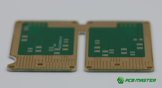
In the world of printed circuit boards (PCBs), thickness plays a crucial role in performance and durability. Thick PCBs, typically defined as those exceeding 3.0mm in thickness, are essential in applications that require high power handling, heat dissipation, and mechanical strength. These include industrial machinery, automotive systems, high-end electronics, and even medical devices. As the demand for more robust and reliable PCB designs grows, the need for thick PCBs has become more prominent.
However, manufacturing thick PCBs presents significant challenges. The increased material thickness affects various stages of the production process, from drilling and shaping to plating and assembly. In this article, we’ll explore the key difficulties involved in producing PCBs thicker than 3.0mm, focusing on mechanical processing, lamination, plating, and soldering. We’ll also provide effective strategies to overcome these challenges and ensure high-quality results. Let’s dive into the complexities of thick PCB manufacturing and the solutions that can help mitigate these issues.
Why Does PCB Thickness Above 3.0mm Pose Manufacturing Challenges?
PCB thickness above 3.0mm poses manufacturing challenges due to increased complexity in drilling, lamination, electroplating, and assembly, requiring specialized equipment and processes to maintain precision and reliability.
What is Thick PCB Manufacturing and What Are the Common Challenges?
Thick PCB manufacturing refers to the production of printed circuit boards that are thicker than 3.0mm. These types of PCBs are used in specialized applications, such as high-power electronics, automotive systems, and industrial equipment. Manufacturing thick PCBs presents unique challenges due to their increased material thickness. The primary issues involve mechanical processing, lamination, plating, and assembly, all of which become more complex as the thickness increases.
The increased thickness impacts every stage of production. For example, drilling deeper holes becomes difficult because the tools have to work through more material. The lamination process also becomes harder, as thick boards tend to warp due to uneven heat distribution. Additionally, the electroplating process struggles with deeper holes, leading to uneven copper coating. All these factors make it harder to achieve the precision and reliability that thicker PCBs demand.
In short, manufacturing thick PCBs requires highly specialized equipment and processes, as well as greater attention to detail and more stringent quality control measures.
Technical Differences Between Various PCB Thicknesses (3.0mm, 4.0mm, 6.0mm, and Beyond)
The technical challenges of producing PCBs grow as their thickness increases, with each thickness level introducing specific issues.
3.0mm PCBs: At this thickness, manufacturers start facing issues like drilling difficulties and slight warping during the lamination process. However, the challenges are still manageable with standard equipment and techniques.
4.0mm PCBs: At 4.0mm, the challenges become more pronounced. The deeper drilling required for vias and through-holes leads to higher risks of drill bit wear and poor hole quality. Additionally, lamination becomes more complicated as the inner layers may not bond correctly, leading to weaker layer adhesion.
6.0mm PCBs and Thicker: Beyond 6.0mm, manufacturing becomes significantly more difficult. Deep-hole drilling is prone to defects like broken drill bits and misaligned holes. The lamination process also faces issues with heat dissipation, making it harder to maintain uniform pressure during pressing, which can result in board warping. Additionally, electroplating challenges intensify due to the difficulty of coating deep holes evenly, resulting in uneven copper distribution.
The thicker the PCB, the more specialized equipment and advanced techniques are required, which increases production costs and complexity.
What Are the Major Challenges in Manufacturing Thick PCBs?
The major challenges in manufacturing thick PCBs include difficulties in drilling, lamination, plating, soldering, and handling specialized materials and equipment, all of which become more complex as the board thickness increases.
1. Mechanical Processing Challenges
Drilling Problems:
Drilling is one of the most difficult processes when it comes to thick PCBs. As the board thickness increases, drilling deeper holes becomes a challenge for several reasons:
l Increased Hole Depth & Chip Removal Difficulty: With thicker boards, drill bits have to work through more material, which makes it harder to remove chips and debris. This leads to higher friction, increased heat, and a greater chance of drill bits wearing out or breaking.
l High Aspect Ratio Leads to Misalignment: Thicker boards often require deeper holes. When the ratio of hole depth to diameter (known as aspect ratio) becomes too large, drill bits are more likely to drift off course, leading to misaligned holes. This causes poor hole positioning, which can disrupt the assembly process.
l Poor Hole Wall Quality & "Bellmouth" Effect: Deeper holes in thick PCBs often result in rough hole walls or an undesirable widening of the hole at the opening (also known as the "bellmouth" effect). This can compromise the integrity of the hole and affect the overall board quality.
Shaping Problems:
l V-Cut Failure & Edge Chipping: The traditional V-cut method used for board separation may fail for thicker PCBs. The cutting depth is limited, and forcing the cut too deep can lead to chipped edges, cracks, or even breakage. This is especially problematic when precision is essential for the final product.
l Difficult Milling & Faster Tool Wear: Milling thicker boards requires more force, which accelerates the wear on milling tools. As the tools dull, they become less effective, leading to a decrease in production quality and an increased frequency of tool replacements.
2. Lamination and Thermal Stress Control Challenges
Insufficient Resin Filling:
In thicker PCBs, the distance between layers increases, which can result in insufficient resin flow during the lamination process. This issue occurs because the resin, used to bond the layers, may not flow evenly to fill the gaps, leading to poor layer adhesion. This weak bond between the layers can cause the PCB to fail during operation, especially under stress.
Bubbles and Layer Separation:
During the high-temperature, high-pressure lamination process, gases and volatile substances within the materials are trapped, leading to the formation of bubbles. These bubbles cause layer separation or weak points in the PCB, reducing its reliability. High-quality thick PCBs require precise control over the lamination process to ensure that all air is evacuated, and the layers bond effectively.
Warpage and Deformation:
As different materials are used in PCB manufacturing (e.g., copper foil, prepreg, and core material), they have different coefficient of thermal expansion (CTE). When the PCB is heated during lamination and then cooled, the materials expand and contract at different rates, leading to warping or deformation. This issue is more pronounced in thicker PCBs and can make the boards unsuitable for certain applications, such as precise surface-mount technology (SMT) assembly.
3. Electroplating Challenges
Copper Plating Uniformity Issues:
When plating deeper holes in thick PCBs, there is a risk of poor copper coating distribution. The issue, known as the "dogbone" effect, occurs when the plating in the center of the hole is thinner than at the edges. This results in uneven copper thickness, which can affect the electrical performance and reliability of the PCB.
Filling Blind and Buried Holes:
Thick PCBs often have blind or buried vias (holes that do not go through the entire board). These holes are more difficult to fill with copper during electroplating. If the vias are not properly filled, it can affect signal transmission and reduce the PCB's electrical capacity, making it unsuitable for high-frequency or high-power applications.
4. Through-Hole Insertion and Soldering Problems
Poor Solder Wetting (Solder "Wicking" Issues):
In thick PCBs, through-hole components (such as resistors or capacitors) are more difficult to solder due to the increased material thickness. Solder wicking refers to the inability of the solder to adequately penetrate the hole, leading to insufficient solder joint formation. This issue can create weak connections, increasing the risk of failure under mechanical stress or heat.
Component Mounting Problems:
For heavy components mounted on thick PCBs, solder joints are put under more stress due to the weight and mechanical forces. These components may suffer from fatigue and eventually fracture the solder joints, leading to component failure. Special care must be taken in designing the PCB to handle the weight of the components and ensure secure mounting.
5. Equipment and Material Limitations
Equipment Compatibility:
Many automated manufacturing systems, including conveyor systems, exposure machines, and etching lines, have limitations on the maximum board thickness they can handle. For instance, some systems are not designed to handle PCBs thicker than 3.2mm, meaning additional investment or process adjustments are needed for thicker boards. This increases both the complexity and cost of production.
Material Requirements:
Thicker PCBs require high-performance materials, such as high-Tg (glass transition temperature) and low-CTE (coefficient of thermal expansion) substrates. These materials can better withstand thermal stresses during the production process but come at a higher cost. Moreover, using these specialized materials adds complexity to the manufacturing process, making it more expensive and difficult to achieve high yields.
How to Overcome Manufacturing Challenges for PCBs Over 3.0mm Thickness?
To overcome manufacturing challenges for PCBs over 3.0mm thickness, optimize drilling and shaping techniques, improve lamination processes, upgrade electroplating methods, collaborate closely during design and manufacturing, and implement strict quality control measures.
1. Optimizing Mechanical Processing Techniques
Drilling Optimization:
To tackle drilling difficulties in thick PCBs, manufacturers can adopt several techniques to improve precision and reduce tool wear:
l Step Drilling (Peck Drilling): This technique involves drilling in stages, allowing the drill bit to retreat and clear debris after each pass. This helps reduce heat buildup, prevent drill bit breakage, and improve hole quality, especially for deep holes.
l Using High-Quality Drill Bits: Employing specialized, high-quality drill bits such as tungsten carbide can improve drilling accuracy and extend tool life. Optimizing drilling parameters like speed and feed rate also helps in reducing friction and tool wear.
l Controlling Aspect Ratio & Using Step Drilling: To avoid misalignment issues, it's crucial to keep the hole’s aspect ratio (depth-to-diameter ratio) within recommended limits (typically less than 10:1). Using step drilling with progressively larger drill bits can help ensure better hole accuracy and minimize the risk of drift.
Shaping Optimization:
l Abandoning V-Cut & Switching to Routing: For thick PCBs, the traditional V-Cut method becomes inefficient, especially for cuts deeper than 2/3 of the board thickness. Instead, routing or stamp hole techniques can be used, which allows for more precise and deeper cuts without compromising the board’s integrity.
l Slow Milling and Multi-Pass Milling: Slowing down the milling process and using multiple passes allows for smoother cuts and reduces the wear on milling tools. This approach also helps achieve higher precision in shaping thick PCBs.
2. Improving Lamination Process
Resin Filling:
Proper resin flow is essential for ensuring good layer adhesion in thick PCBs. Manufacturers can address resin filling issues through the following methods:
l Using High-Resin Content PP Sheets: Selecting prepreg sheets with higher resin content helps to ensure sufficient resin flow during the lamination process, even in thick boards. This helps avoid voids and air gaps between layers.
l Multi-Stage Temperature Pressing: Implementing a multi-stage temperature pressing process ensures that the resin has enough time to flow and fill the gaps between layers, allowing for better bonding. The process starts at lower temperatures to allow resin movement before applying high pressure to cure the board.
l Using Buffer Materials & Flow Channels: Adding buffer materials and creating resin flow channels along the edges of the PCB during lamination can help guide excess resin and trapped air out of the board, ensuring better adhesion and preventing delamination.
Reducing Warping:
Post-Lamination Baking: After lamination, it’s crucial to bake the PCB to remove internal stress. A baking process helps relieve thermal strain, reducing warping and ensuring that the PCB stays flat during subsequent manufacturing stages.
3. Upgrading Electroplating Techniques
Pulse and Horizontal Electroplating:
l Pulse Electroplating: This technique improves copper deposition uniformity in deep holes. It involves periodically switching the current on and off, which enhances the exchange rate of the plating solution and ensures even copper thickness, reducing the "dogbone" effect.
l Horizontal Electroplating: This method uses a horizontal plating system to better control copper distribution within deep holes. It ensures that the plating solution is evenly distributed, preventing areas of thin copper on the inside of the hole.
Enhanced Stirring and Ultrasonic Vibration:
l Ultrasonic Vibration: To improve plating uniformity in deep holes, ultrasonic agitation can be applied. This helps the plating solution penetrate deeper into holes and ensures that the copper is deposited evenly throughout the entire hole.
Extended Electroplating Time:
l Longer Plating Time: Extending the plating time allows the copper to build up evenly within deep vias and holes, ensuring that the copper thickness meets the required standards for electrical and mechanical performance.
4. Optimizing Design and Manufacturing Collaboration
Design Stage:
l Relax Design Tolerances: When designing thick PCBs, it’s beneficial to increase the clearance between lines and pads, and optimize hole sizes. This reduces the complexity of the manufacturing process, making it easier to achieve consistent quality in production.
l Back Drilling to Optimize Signal Quality: For high-speed signals, using back drilling to remove unused copper from through-holes (called "stubs") can reduce signal interference and improve electrical performance, especially in thick PCBs.
Manufacturing Stage:
l Adding Process Margins and Locator Holes: During manufacturing, adding extra process margins and locator holes can help improve the precision of the alignment and positioning. These adjustments make it easier to handle the thick boards during the drilling, routing, and plating processes, reducing the risk of misalignment.
5. Strict Quality Control and Inspection
Electrical Continuity Testing:
l 100% Electrical Testing: Every thick PCB should undergo electrical continuity testing to ensure that all circuits are correctly connected. This is particularly important in thick PCBs, where vias and connections may be more difficult to inspect manually.
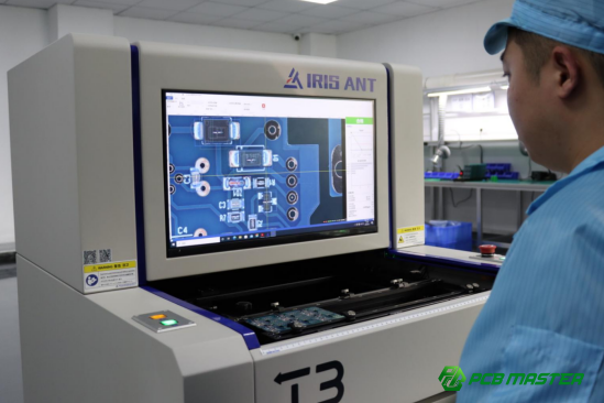
Cross-Sectional Analysis & 3D X-Ray Inspection:
l Cross-Sectional Analysis: Regularly conducting cross-sectional analysis allows manufacturers to check the quality of the plating, the layer adhesion, and other critical features. It also helps identify internal defects early in the process.
l 3D X-Ray Inspection: For deep vias or buried holes, 3D X-ray can be used to examine the internal structure of the PCB. This non-destructive technique allows for a detailed view of hole quality, layer alignment, and overall manufacturing integrity.
Thermal Stress Testing:
l High-Temperature Soldering Tests: To ensure the reliability of thick PCBs, conducting high-temperature soldering tests (like immersion in molten solder at 288°C) is essential. This helps assess the strength of solder joints and the PCB's ability to withstand high temperatures during operation.
Common Misconceptions and Issues in Thick PCB Manufacturing
Common misconceptions in thick PCB manufacturing include assuming conventional processes can handle all thicknesses, while issues like the "dogbone" effect in electroplating, poor solderability, and warping often arise due to inadequate methods and material challenges.
Misconception: Believing Conventional Processes Can Handle All Thick PCB Manufacturing
A common misconception in thick PCB manufacturing is assuming that traditional processes designed for standard, thinner PCBs can also be used for thicker boards. While conventional methods may work for boards up to 3.0mm, thicker boards require specialized techniques due to the increased complexity in drilling, lamination, and plating. Using standard equipment and methods on thick boards often leads to poor hole quality, inconsistent plating, warping, and decreased reliability.
For instance, using traditional V-Cut methods for thick PCBs may lead to edge chipping or even board breakage due to the deeper cuts required. Likewise, standard drilling techniques may result in drill bit breakage or misaligned holes in thick boards, impacting overall PCB performance. Adapting the process and using appropriate equipment and methods designed for thicker PCBs are crucial to ensure manufacturing success.
Common Issue 1: "Dogbone" Effect in Electroplating
The "dogbone" effect refers to an issue during electroplating where copper is deposited unevenly within deep vias in thick PCBs. This phenomenon occurs when the plating solution cannot reach the center of the hole, resulting in thicker copper on the hole's edges and a much thinner layer in the center. The result is a weak connection and compromised electrical performance. The dogbone effect can lead to failures in high-power or high-frequency applications, as the PCB may not conduct electricity properly or could even experience open circuits.
To address this, pulse electroplating or horizontal electroplating methods can be used to improve plating uniformity, ensuring that copper is evenly distributed throughout deep vias.
Common Issue 2: Poor Solderability and Inadequate Solder Penetration
Another challenge in thick PCB manufacturing occurs during the soldering process, especially when dealing with through-hole components. Poor solderability often arises because solder cannot adequately penetrate deep holes, a problem exacerbated in thick PCBs. As a result, poor solder joints are formed, leading to weak electrical connections and potential mechanical failure.
In particular, wave soldering and hand soldering can struggle to fully wet the solder within deeper vias. This leads to issues such as cold solder joints, poor conductivity, and the risk of solder joint failure under mechanical or thermal stress. To resolve this, manufacturers may need to employ reflow soldering with more advanced fluxes or use pre-heating techniques to improve the solder’s ability to reach all areas of the hole.
Common Issue 3: Warping and Deformation During Manufacturing
Warpage is a frequent issue when manufacturing thick PCBs. This occurs due to the differences in the thermal expansion coefficients (CTE) of various materials used in the PCB, such as copper, prepreg, and the core material. As the PCB is heated during the lamination process and then cooled, these materials expand and contract at different rates, leading to deformation or bending of the board.
Warpage is especially problematic in Surface-Mount Technology (SMT) assembly, where precise placement of components is critical. Warped boards can make it difficult to align the components properly, leading to poor solder joints and reliability issues in the final product. To combat this, manufacturers often use multi-stage curing processes and post-baking techniques to reduce internal stresses and maintain a flat board shape.
Conclusion
Manufacturing thick PCBs requires overcoming a range of challenges, including difficulties with drilling, electroplating, soldering, and warping. As the thickness of the board increases, so do the complexities in achieving high precision and reliable performance. These obstacles demand specialized techniques, advanced equipment, and a deep understanding of the materials and processes involved.
This is where PCBMASTER comes in. As an experienced PCB and PCBA supplier, we are dedicated to delivering high-quality products, including thick PCBs, with exceptional precision and performance. With years of expertise, we utilize cutting-edge technologies to address the unique challenges of thick PCB manufacturing, ensuring that every project meets the highest standards. Whether you require standard PCBs or high-performance thick boards, PCBMASTER is your reliable partner for quality solutions. Contact us today to discover how we can support your needs and help bring your designs to life.
FAQs
How Does the Drilling Difficulty Increase When PCB Thickness Exceeds 3.0mm?
As PCB thickness increases beyond 3.0mm, drilling becomes more challenging due to the increased drilling depth. This deeper drilling leads to several issues:
l Chip Removal Difficulty: The longer the hole, the harder it is for the drill to effectively remove debris (chips). This increases friction, raises temperatures, and puts extra strain on the drill bit.
l Drill Bit Breakage: With increased resistance and friction, the drill bits are more likely to break during the process, especially in deeper holes. This not only affects efficiency but can also damage the PCB material.
l Hole Misalignment: As the hole depth-to-diameter ratio (aspect ratio) increases, the drill bit may drift, causing misalignment of the hole. This can result in inaccurate hole positioning, leading to issues in multi-layer PCB alignment and overall functionality.
To address these challenges, advanced drilling techniques like peck drilling (step drilling) and using high-quality, durable drill bits are recommended to ensure precise and efficient drilling.
How Does Inadequate Resin Filling in Thick PCBs Affect Manufacturing Quality?
In thick PCBs, resin filling during lamination is crucial for strong layer bonding. If the resin does not fully fill the space between the layers, it leads to a number of issues:
l Void Formation: Insufficient resin flow can create air pockets or voids within the PCB, particularly in the inner layers. This weakens the structural integrity of the board and can cause delamination or layer separation.
l Reduced Layer Adhesion: Proper resin filling ensures strong adhesion between layers. Without it, the layers might not bond well, leading to reduced layer-to-layer strength, which affects the PCB’s overall reliability, especially under mechanical stress or temperature fluctuations.
To avoid this, it’s important to use high-resin content prepreg sheets and employ multi-stage temperature pressing to ensure adequate resin flow during lamination.
How Can the "Dogbone" Effect in Electroplating of Thick PCBs Be Solved?
The "dogbone" effect in electroplating occurs when copper plating is uneven, often resulting in thicker copper deposits at the edges of a deep hole, and thinner copper or even no copper in the center of the hole. This issue compromises electrical conductivity and can lead to open circuits or weak connections. To overcome this challenge:
l Pulse Electroplating: Pulse plating helps by periodically switching the current on and off, which enhances the flow of plating solution and helps copper reach the center of deep vias more effectively, ensuring uniform copper thickness across the hole.
l Horizontal Electroplating: In horizontal electroplating, the plating solution is evenly distributed across the PCB, which improves penetration into deep vias and leads to more consistent copper deposition.
l Ultrasonic Vibration: Adding ultrasonic agitation to the plating process helps further enhance the plating solution’s penetration into deep vias, improving copper uniformity and reducing the dogbone effect.
By implementing these advanced electroplating methods, manufacturers can achieve uniform copper deposition and ensure long-term reliability.
How Can Warping in Thick PCBs Be Reduced?
Warping occurs when different materials in the PCB expand or contract at different rates due to thermal stress during manufacturing. In thick PCBs, this is more pronounced and can lead to misalignment or difficulties during SMT (Surface Mount Technology) assembly. To minimize warping:
l Extended Low-Temperature Holding: During lamination, extending the low-temperature holding time allows the resin to flow better and helps release trapped gases. This reduces internal stress and the likelihood of warping during the heating and cooling phases.
l Post-Baking Process: After the lamination process, applying a post-baking procedure helps to remove residual internal stresses by subjecting the PCB to a controlled, gradual heating process.
l Material Selection: Choosing materials with low CTE (Coefficient of Thermal Expansion), such as high-Tg substrates, can help minimize the difference in expansion rates between layers, reducing the chances of warping.
Together, these techniques ensure that the PCB remains flat and stable throughout the manufacturing process, improving the accuracy of component placement during SMT.
Why Is Early Communication with Manufacturers Important for Thick PCB Production?
Early communication with PCB manufacturers is critical for thick PCB production due to the following reasons:
l Complex Manufacturing Process: Thick PCBs come with unique challenges, such as deeper drilling, specialized lamination processes, and higher material costs. Early collaboration ensures the design is optimized for these challenges and allows manufacturers to plan for any potential issues upfront.
l Increased Production Costs and Time: Thick PCBs generally require more time and higher costs due to the additional processes involved. By discussing these aspects early, manufacturers can set realistic expectations and ensure timely delivery without unexpected delays or costs.
l Avoiding Design and Manufacturing Discrepancies: If manufacturers and designers don’t communicate early, there may be mismatches between the design intent and the manufacturing feasibility. Early discussions help prevent misalignments and ensure the design is optimized for production.
Overall, early communication allows for smoother production and ensures the final product meets the required specifications, improving efficiency, quality, and cost-effectiveness.
Author Bio
Hi, I'm Carol, the Overseas Marketing Manager at PCBMASTER, where I focus on expanding international markets and researching PCB and PCBA solutions. Since 2020, I've been deeply involved in helping our company collaborate with global clients, addressing their technical and production needs in the PCB and PCBA sectors. Over these years, I've gained extensive experience and developed a deeper understanding of industry trends, challenges, and technological innovations.
Outside of work, I'm passionate about writing and enjoy sharing industry insights, market developments, and practical tips through my blog. I hope my posts can help you better understand the PCB and PCBA industries and maybe even offer some valuable takeaways. Of course, if you have any thoughts or questions, feel free to leave a comment below—I'd love to hear from you and discuss further!