


What is PCB Plated Via Plugging? A Complete Guide for Electronics Designers
PCB (Printed Circuit Board) manufacturing is the foundation of most electronic devices, ranging from smartphones to medical equipment. In PCB design, vias are small holes drilled into the board to connect different layers of circuits. These vias help transmit signals and power between layers, ensuring the functionality of the device. However, there are instances when vias need to be filled or sealed to improve the overall performance and reliability of the PCB. This is where PCB Plated Via Plugging comes in.
Understanding PCB Plated Via Plugging is crucial for electronics designers because it enhances the quality and durability of the final product. By filling or plugging vias, designers can prevent issues like signal interference, reduce the potential for electromagnetic noise, and enhance the structural integrity of the PCB. This process ensures the board functions efficiently, especially in high-frequency or high-reliability applications.
This guide will provide a comprehensive understanding of PCB Plated Via Plugging, its importance in PCB design, and the steps involved in the process. By the end of this article, you'll have a clear grasp of how via plugging can elevate your PCB designs, ensuring optimal performance and longevity.
What is PCB Plated Via Plugging?
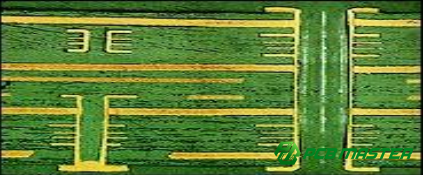
PCB Plated Via Plugging refers to the process of filling or sealing the vias (small holes) in a PCB with a material, typically to prevent them from being electrically conductive. Vias are essential in PCB design as they provide electrical connections between different layers of the circuit. However, sometimes it is necessary to fill or block certain vias to improve the board’s performance, reduce interference, and enhance its structural strength. Via plugging involves inserting a filler material into these holes and then applying a plating layer on top, creating a smooth, sealed surface. This prevents unwanted electrical signals from traveling through the vias, particularly in high-frequency or sensitive designs.
Description of how vias are used in PCB design
Vias in PCB design serve as channels that connect various layers of a PCB, enabling electrical signals to pass between them. There are several types of vias, such as through-hole vias, blind vias, and buried vias, depending on their placement within the layers. Without vias, it would be impossible to create multi-layer PCBs, which are common in most modern electronic devices. However, in certain situations, such as when vias are no longer needed for functionality or when they could negatively affect signal integrity, vias may be filled or plugged.
Materials used for via plugging
The materials used for PCB via plugging vary, depending on the design requirements. One common material is epoxy resin, a non-conductive material that fills the vias and hardens to seal them completely. Copper plating is often used to finish the surface after the via has been filled, ensuring that the board has a smooth and uniform finish. In some cases, solder or conductive adhesives are used for plugging, especially when the vias need to maintain electrical continuity. The choice of material depends on the type of PCB, its intended use, and the performance requirements of the device.
Why is PCB Plated Via Plugging Important for PCB Design?
PCB Plated Via Plugging is important for PCB design because it improves signal integrity, enhances mechanical strength, and ensures reliable performance while reducing manufacturing complexities and costs.
How PCB Plated Via Plugging affects signal integrity
PCB Plated Via Plugging plays a crucial role in improving signal integrity by minimizing unwanted electrical interference. Interference and noise can be caused when signals travel through vias that are not properly sealed. If a via is left open or unfilled, it can create a pathway for noise or electromagnetic interference (EMI) to affect the circuit. By plugging these vias with non-conductive materials like epoxy resins, the flow of unwanted signals can be blocked, ensuring cleaner signal transmission and enhancing overall PCB performance. For example, in high-speed circuits where precision matters, even small amounts of interference can degrade performance, making via plugging essential.
Moreover, crosstalk—the unwanted transfer of signals between different circuit paths—can be reduced significantly by filling vias. Vias that are improperly filled or exposed could become a medium for crosstalk, leading to issues such as signal degradation. By plugging these vias, the likelihood of crosstalk between layers is reduced, helping maintain a stable and reliable electrical connection between different parts of the PCB.
Enhanced reliability and mechanical strength
Via plugging also improves the mechanical strength and durability of a PCB. The filling material used in via plugging acts as a solid barrier, preventing stress or damage to the vias during handling, soldering, or thermal cycling. A plugged via adds additional structural integrity, ensuring that the PCB can withstand harsh environments and physical stress.
This is particularly important in high-reliability applications such as aerospace or medical devices, where the PCB must function flawlessly over a long period. In these industries, failure is not an option, and a plugged via can help ensure the board remains intact and free from cracks or shorts that could affect performance. For instance, in an aerospace application, the PCB might be subjected to extreme conditions (temperature changes, vibration). Via plugging ensures the PCB remains robust and resistant to damage, thus increasing the overall reliability of the device.
Impact on manufacturability and cost
PCB Plated Via Plugging can streamline the PCB manufacturing process by simplifying the design. When vias are plugged, it reduces the need for complex routing or multiple layers of interconnections, helping to save time and resources during production. Furthermore, via plugging can improve the yield during manufacturing by preventing common defects like open or shorted vias.
However, cost implications can vary. For low-volume designs, via plugging may add an additional step to the manufacturing process, increasing the cost of production. This is due to the added materials and labor required for the plugging process. On the other hand, for high-volume designs or complex PCBs, the benefits of reduced defects and improved signal integrity can outweigh the extra costs. Designers need to balance the cost of plugging with the performance benefits and reliability required for the specific PCB application.
By incorporating via plugging into the design, manufacturers can optimize their production efficiency, minimize potential errors, and ensure the final product meets high-quality standards, which is especially valuable for industries where performance is critical.
How Does the PCB Plated Via Plugging Process Work?
The PCB Plated Via Plugging process involves drilling vias, copper plating them for conductivity, filling the vias with materials like epoxy resin or solder, curing or reflowing the fill material, and applying a final layer of copper to seal the vias and ensure non-conductivity.
Step-by-step explanation of the via plugging process
The PCB Plated Via Plugging process involves several stages that work together to fill and seal vias, ensuring the PCB is both electrically and mechanically stable.
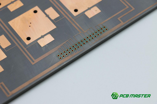
1. Drilling: The first step in the process is drilling small holes, known as vias, into the PCB to create electrical connections between different layers. These vias are created according to the design specifications using a drilling machine, which accurately places the holes in precise locations.
2. Copper Plating: After drilling, the vias are plated with copper. Copper plating is essential because it provides conductivity to the vias, allowing electrical signals to pass through them. This step involves depositing a thin layer of copper on the walls of the vias using an electroplating process.
3. Filling the Vias: Once the vias are copper-plated, they are filled with a material, usually an epoxy resin or sometimes solder. The filling material ensures that the vias no longer conduct electricity, which is especially useful for isolating specific layers. The material is injected into the vias, either manually or using automated systems, ensuring they are completely filled.
4. Reflow or Curing: After the vias are filled with the resin or solder, they need to be cured or hardened. For epoxy resins, this typically involves a curing process in an oven where the temperature is controlled to allow the resin to harden and adhere firmly to the via walls. For solder, a reflow process is used to melt and then solidify it, ensuring the filled vias maintain their integrity.
5. Final Copper Plating: After the via is filled and hardened, a final layer of copper is applied to make the filled vias non-conductive. This step ensures the vias are smooth and ready for further manufacturing or assembly. The copper plating also adds structural support to the PCB, improving its overall durability.
Tools and equipment used in the via plugging process
Several tools and machines are essential in the PCB via plugging process, ensuring that each step is performed accurately and efficiently:
l Key Machinery Involved: Machines such as drilling machines (for creating vias), plating tanks (for copper plating), and curing ovens (for resin hardening) are necessary for the various steps. Automated machines can handle much of the process, ensuring consistency and precision. Injection systems are used to fill the vias with resin or solder, while reflow ovens or curing chambers are used to set the fill material.
l Role of Automation in the Process: Automation plays a crucial role in modern PCB manufacturing. Automated systems ensure that vias are drilled accurately, the filling material is injected without air bubbles, and the curing or reflow processes are performed consistently. This reduces human error and increases production efficiency, especially in high-volume manufacturing.
l Types of Resins and Materials Used for Plugging: The primary materials used for via plugging are epoxy resins (which are non-conductive and provide good mechanical strength) and solder (used when conductive vias are needed). The choice of material depends on the application and the desired properties of the PCB. For instance, in high-frequency applications, non-conductive epoxy resins are preferred to minimize signal interference. Some advanced applications may also use polymer-based materials or specialized conductive adhesives for filling vias.
By understanding these key steps and tools, PCB designers and manufacturers can effectively use via plugging to improve the performance, reliability, and manufacturability of their PCBs.
What Are the Benefits of PCB Plated Via Plugging?
PCB Plated Via Plugging offers benefits such as reduced electromagnetic interference (EMI), improved signal integrity in high-frequency applications, enhanced PCB reliability and durability, increased board density, and cost-effectiveness in manufacturing.
Reduction of electromagnetic interference (EMI) and signal noise
PCB Plated Via Plugging is essential for reducing electromagnetic interference (EMI) and signal noise. When vias are left unfilled, they can act as unwanted antennas, picking up or transmitting electromagnetic signals that interfere with the circuit’s intended signals. This can lead to signal distortion or even malfunction in sensitive applications. By plugging the vias with non-conductive materials like epoxy resin, these interference pathways are blocked, resulting in cleaner signals and better overall performance.
In comparison, unfilled vias often allow electrical noise to flow through the PCB, leading to degraded signal integrity, particularly in high-speed or high-frequency circuits. Plugging these vias provides a shielding effect, significantly improving the PCB's resistance to EMI. For example, in communication devices where signal clarity is crucial, plugging vias helps maintain high-quality, stable signals across the board.
Improved performance in high-frequency applications
Via plugging plays a key role in enhancing performance in high-frequency applications. When vias are unfilled, they can create unwanted signal paths, affecting the quality of high-frequency signals. Plugging the vias eliminates these paths, helping maintain signal integrity.
By plugging vias, impedance mismatches—which occur when signals experience resistance while traveling through a circuit—can be minimized. These mismatches often lead to signal reflection or loss of signal strength. With plugged vias, the signal flow is smoother, which is especially important for high-speed signal transmission, such as in telecommunications or high-frequency computing devices. Plugging vias ensures that signals pass through layers without disruptions, improving both speed and reliability in applications like RF circuits and high-speed processors.
Enhanced PCB reliability and durability
Via plugging improves the long-term reliability and durability of a PCB. The filling material in the vias acts as a protective barrier, preventing mechanical stress or environmental damage from affecting the circuit.
As PCBs age, the unfilled vias can become vulnerable to physical damage or moisture ingress, which could cause shorts or failures. By filling the vias, manufacturers add structural strength to the PCB, increasing its resistance to thermal cycling and vibration. This is particularly important in high-reliability sectors like aerospace, automotive, and medical devices, where the PCB needs to endure extreme conditions. A plugged via helps the PCB maintain its performance over its entire lifecycle, reducing the risk of failure under stress.
Increased board density and simplified routing
Via plugging also helps in increasing board density and simplifying routing. In modern PCBs, space is often limited, and routing can be complex. By plugging unnecessary vias, designers can free up valuable space, allowing for more components or additional layers on the board. This is especially beneficial in compact designs, like in smartphones or wearable electronics, where every square millimeter counts.
By reducing the number of vias and optimizing the layout, designers can achieve better layer stack-ups and use shorter traces, leading to improved performance and less signal degradation. In cases where additional layers are required, via plugging creates more room for routing, which can optimize the overall design while maintaining performance and reducing the PCB's overall size.
Cost-effectiveness in specific applications
Via plugging can be cost-effective in certain PCB applications, especially in high-volume or complex designs. For example, filling vias can help avoid the need for expensive high-frequency materials or complex routing techniques that would otherwise be required to mitigate the impact of unfilled vias. Additionally, plugged vias help reduce defects and yield loss during manufacturing, leading to fewer faulty units and ultimately lower costs in the production process.
For large-scale PCB manufacturers, the benefits of plugged vias, such as improved signal quality and reduced need for additional layers, can lead to cost savings in both manufacturing and assembly. While via plugging may incur some upfront costs, particularly in low-volume production, it can ultimately save money by reducing defects, enhancing yield, and improving product performance over time.
What Are the Types of Via Plugging Methods Used in PCB Manufacturing?
The types of via plugging methods used in PCB manufacturing include standard via plugging, conductive via plugging, non-conductive via plugging, and the choice between filled and unfilled vias, each serving different design and performance needs.
Standard via plugging
Common methods and materials
Standard via plugging is the most commonly used method in PCB manufacturing. In this process, vias are filled with non-conductive materials such as epoxy resins or polymer-based compounds. These materials fill the vias, blocking any electrical flow and creating a smooth surface for further manufacturing. The epoxy used in standard via plugging is typically chosen for its durability, resistance to environmental factors, and ease of application.
Overview of the process used in most designs
The standard via plugging process involves drilling the vias, copper plating the holes for conductivity, and then filling them with a resin. The process is followed by curing the resin to harden it, ensuring that the vias are sealed properly. After curing, the filled vias are usually plated again to provide a smooth and finished surface. This method is widely used in most multi-layer PCBs as it enhances board strength and reduces the risk of electrical shorts between layers.
Conductive vs. Non-conductive via plugging
Differences in materials and applications
There are two primary types of via plugging based on the materials used: conductive and non-conductive.
l Conductive via plugging uses materials like conductive epoxy or solder, which maintain electrical conductivity through the via, ensuring that the via still functions as an electrical path. This method is typically used in designs where a continuous electrical connection is needed across the vias.
l Non-conductive via plugging, on the other hand, uses materials like insulating epoxies or resins to block electrical current, making the vias non-functional for electrical connections. This type is commonly used in designs that require isolation between layers or where the vias should not transmit signals.
When to use conductive plugging vs. non-conductive
l Conductive via plugging is best for high-frequency designs or when the via needs to continue carrying signals or power between layers.
l Non-conductive via plugging is ideal for high-speed circuits, where isolating specific layers or avoiding unwanted interference is crucial. Non-conductive plugging helps prevent crosstalk and interference in sensitive parts of the PCB, such as RF circuits or signal processing areas.
Filled vs. unfilled vias in different types of PCBs
What’s the difference between a via that is only filled with resin and one that is fully plated and filled?
Filled vias are completely filled with materials like resin or solder, preventing electrical conductivity. Unfilled vias are drilled holes that may remain empty or filled only partially, leaving room for possible signal flow. A filled via ensures that the hole does not interfere with the board's electrical performance, while unfilled vias could still potentially allow unwanted signals or noise to pass through.
In contrast, plated vias undergo copper plating after filling, ensuring that the via is properly sealed with a non-conductive surface. A via that is fully plated and filled has both the filling material and an additional layer of copper plating, making it smooth, stable, and non-conductive. This method is used for enhanced insulation and cleanliness in high-density designs.
When to choose filled vias in high-frequency designs versus non-plated or standard vias
In high-frequency designs, filled and plated vias are preferred because they minimize noise, interference, and signal distortion. The non-conductive filling material and copper plating provide excellent insulation, making it ideal for sensitive signal paths. Unfilled vias or non-plated vias should be avoided in high-frequency applications as they can introduce impedance mismatches, noise, and unwanted signal paths.
Comparison table
Feature Standard Via Plugging Conductive Via Plugging Non-conductive Via Plugging Filled vs. Unfilled Vias Material Used Epoxy resin, polymer-based compounds Conductive epoxy, solder Insulating epoxy, resins Resin, solder (filled) / Empty (unfilled) Electrical Conductivity Non-conductive Conductive Non-conductive Conductive (unfilled) / Non-conductive (filled) Applications General PCB designs High-speed or power circuits High-frequency, noise-sensitive designs High-density designs (filled); general designs (unfilled) Performance in High-frequency Good, with effective insulation Essential for signal or power paths Best for isolating layers, avoiding interference Filled vias reduce signal noise; unfilled may allow interference Cost and Complexity Lower cost and complexity Higher cost, requires precise control Similar cost to non-conductive, but more specialized Filled vias more expensive; unfilled vias easier to manufacture
| Feature | Standard Via Plugging | Conductive Via Plugging | Non-conductive Via Plugging | Filled vs. Unfilled Vias |
| Material Used | Epoxy resin, polymer-based compounds | Conductive epoxy, solder | Insulating epoxy, resins | Resin, solder (filled) / Empty (unfilled) |
| Electrical Conductivity | Non-conductive | Conductive | Non-conductive | Conductive (unfilled) / Non-conductive (filled) |
| Applications | General PCB designs | High-speed or power circuits | High-frequency, noise-sensitive designs | High-density designs (filled); general designs (unfilled) |
| Performance in High-frequency | Good, with effective insulation | Essential for signal or power paths | Best for isolating layers, avoiding interference | Filled vias reduce signal noise; unfilled may allow interference |
| Cost and Complexity | Lower cost and complexity | Higher cost, requires precise control | Similar cost to non-conductive, but more specialized | Filled vias more expensive; unfilled vias easier to manufacture |
This detailed comparison and explanation of via plugging methods provide a clear understanding of the various types used in PCB manufacturing, their materials, applications, and benefits. By selecting the right method based on the specific needs of the design, PCB manufacturers can ensure better performance, reliability, and cost-efficiency.
How to Choose the Right Via Plugging Solution for Your PCB Design?
To choose the right via plugging solution for your PCB design, consider factors like design complexity, signal frequency requirements, cost versus performance trade-offs, and the specific challenges of space constraints and signal integrity.
Key factors to consider when selecting via plugging methods
When selecting the right via plugging method for your PCB design, several factors need to be taken into account to ensure the most effective and cost-efficient solution.
l Design complexity and PCB layer count: The more complex your design and the higher the number of layers, the more critical via plugging becomes. For multi-layer PCBs, via plugging helps improve layer insulation and signal integrity. In simpler, single-layer designs, via plugging may not be necessary unless the vias are causing structural issues or unwanted electrical paths.
l Signal frequency requirements: If your design deals with high-speed or high-frequency signals, via plugging becomes essential to prevent signal degradation and interference. For instance, non-conductive plugging can help shield sensitive circuits from electromagnetic interference (EMI), ensuring signal clarity and preventing cross-talk. On the other hand, for power or low-frequency applications, conductive plugging might be used to maintain electrical continuity.
l Cost vs. performance trade-offs: Choosing the right via plugging method involves balancing the cost and performance needs of the design. While non-conductive via plugging tends to be cost-effective for high-speed designs, conductive via plugging can be more expensive due to the specialized materials used, but it is necessary for certain applications like high-current paths or power circuits. Designers need to assess the performance requirements and decide how much investment is justified based on the importance of the application.
Common design challenges and how via plugging helps address them
l Space constraints and signal integrity issues: In high-density designs, space is often at a premium, and vias can take up valuable board real estate. Via plugging helps solve this by reducing the need for complex routing, optimizing space for additional components or reducing the number of vias altogether. When space is limited, via plugging can free up room for more critical components and prevent routing errors.
l Balancing between high-density designs and signal noise management: High-density designs often struggle with signal noise and crosstalk between layers. Via plugging helps manage this issue by sealing the vias and preventing unwanted interference. For instance, plugging vias in a dense multi-layer PCB helps to isolate signals and shields the layers from external noise, ultimately improving the overall performance. By using via plugging, designers can maintain the necessary layer count without compromising signal integrity, which is crucial for applications like mobile devices and telecommunications equipment.
Applications where PCB Plated Via Plugging is essential
Via plugging is essential in several industries where PCB performance and reliability are critical.
l Specific industries like automotive, telecommunications, and medical devices: In automotive and telecommunications industries, PCBs are exposed to high vibrations, temperature fluctuations, and electromagnetic interference. Via plugging ensures durability and helps maintain signal clarity in these harsh environments. In the medical device industry, where reliability is paramount, via plugging enhances the PCB’s mechanical strength and ensures it performs consistently, even in critical applications like monitoring systems and implantable devices.
l Case studies or examples of successful via plugging implementation: In the automotive industry, sensor systems for self-driving cars require extremely high reliability. A case study involving an automotive PCB showed that via plugging improved the signal integrity of sensors by isolating critical circuits from noise. Similarly, in telecommunications, 5G base station PCBs often rely on via plugging to handle high-frequency signals, ensuring the equipment remains efficient and interference-free. These case studies demonstrate that proper via plugging can significantly enhance both performance and reliability in complex and demanding environments.
By carefully considering the design challenges, application needs, and cost-effectiveness, PCB designers can select the right via plugging solution that meets both their technical and financial requirements.
How Does PCB Plated Via Plugging Affect PCB Testing and Quality Control?
PCB Plated Via Plugging affects testing and quality control by requiring advanced inspection techniques like X-ray imaging to verify the integrity of filled vias, while emphasizing quality assurance practices and adherence to industry standards to prevent common issues such as poor fills, voids, or cracks.
Testing challenges with plugged vias
When vias are plugged, testing and quality control processes can become more challenging. Plugged vias, especially when filled with resin or solder, can obscure the internal structure of the via, making it harder to verify their integrity.
l Inspection techniques for verifying the integrity of filled vias: Traditional visual inspection methods are often not sufficient for checking the internal integrity of plugged vias. X-ray imaging is commonly used to inspect the filled vias, as it allows manufacturers to view the inner structure and confirm that the via is completely filled without any voids or cracks. This ensures the via is properly sealed and will not cause issues like electrical shorts or structural weaknesses later in the PCB's use.
l Importance of visual inspection and X-ray imaging: While X-ray imaging is critical for checking via filling integrity, visual inspection still plays an important role in detecting surface defects, such as improper resin application or uneven plating. Combining both methods ensures a comprehensive quality check, allowing manufacturers to spot and correct defects before the PCB is shipped.
Role of quality assurance in via plugging
Quality assurance (QA) is crucial to ensure that the via plugging process is performed correctly and that the final PCB meets industry standards.
l Best practices for quality checks during manufacturing: During the PCB manufacturing process, several quality checks should be carried out, including pre-plugging inspections to verify the vias are correctly drilled and copper-plated, resin or solder filling checks, and post-plugging inspections to ensure that the fill material is cured or reflowed properly. Additionally, automated optical inspection (AOI) systems can be used to check for common issues like misalignment or incomplete via filling.
l Importance of standards and certifications (e.g., IPC standards): Adhering to IPC standards (such as IPC-2221 for design or IPC-6012 for performance) ensures that via plugging meets both industry expectations and regulatory requirements. Certifications from recognized bodies help guarantee that the manufacturing process adheres to high-quality benchmarks and reduces the risk of defects in the final product.
Troubleshooting common issues in via plugging
Despite careful planning, some common issues may arise during the via plugging process, affecting the performance of the PCB.
Addressing issues like poor fill, voids, or cracks in the filled vias:
l Poor fill: If the via is not completely filled with resin or solder, it can lead to an incomplete seal, which may cause electrical shorts or weak spots in the PCB. This can be addressed by improving the filling process, ensuring that the correct amount of material is injected and that the vias are properly cured or reflowed.
l Voids: Voids (empty spaces inside the via fill) can occur due to air pockets or incomplete filling. Vacuum-assisted filling or using higher-quality resins can help prevent voids. Voids compromise the mechanical strength and electrical integrity of the PCB, so addressing them early is crucial.
l Cracks: Cracking in filled vias often occurs during the curing process, especially if the temperature is too high or the resin expands unevenly. Thermal cycling during curing must be closely controlled to ensure proper material adhesion and avoid cracking. Regular stress testing can also help detect cracks early.
By focusing on thorough testing, quality assurance, and troubleshooting common issues, manufacturers can ensure that the via plugging process enhances the reliability and performance of the PCB, meeting industry standards and customer expectations.
What Are the Costs Involved in PCB Plated Via Plugging?
The costs involved in PCB Plated Via Plugging include material costs (epoxy resins, copper plating), labor and equipment expenses, and factors such as design complexity, the number of vias, and production scale.
Cost breakdown of via plugging in PCB manufacturing
The cost of via plugging in PCB manufacturing is influenced by several factors, including material, labor, and equipment requirements.
l Material costs (epoxy, copper plating, etc.): The primary materials involved in via plugging are epoxy resins or solder for filling the vias, and copper plating for the initial via lining. Epoxy resins are relatively inexpensive, but high-quality resins can add to the cost. Copper plating, although a standard process, also contributes to material costs. The more complex the via plugging (e.g., using conductive or high-performance resins), the higher the material cost.
l Labor and equipment costs: Labor costs involve skilled technicians managing the drilling, filling, and curing processes. Advanced equipment like X-ray inspection machines for verifying filled vias also adds to costs. Automated systems for high-volume production can reduce labor costs, but initial investment in these systems is expensive. The use of automation in large runs, however, can improve overall efficiency, reducing the per-unit labor cost.
Factors influencing the overall cost of via plugging
Several factors influence the total cost of via plugging in PCB manufacturing:
l Complexity of the design and number of vias: The more vias there are and the more complex the design, the higher the cost. For example, multi-layer PCBs with numerous vias may require additional effort to fill and inspect each via, increasing both material and labor costs. Via plugging for complex designs often involves additional quality control steps to ensure each via is filled and insulated correctly.
l Batch size and scale of production: The scale of production significantly affects the cost per unit. For large production runs, the setup costs are spread across more units, making the cost per PCB lower. However, for small batches, the setup costs remain relatively high per unit, making the via plugging process more expensive for smaller projects. As production volume increases, efficiency improves, and the cost of plugging vias decreases.
Cost-benefit analysis for small vs. large production runs
When comparing small vs. large production runs, efficiency and cost-effectiveness become key considerations.
l Comparing the efficiency and cost-effectiveness for different project sizes: In small production runs, the initial setup costs (for materials, equipment, and labor) may not be amortized over a large enough number of units, making via plugging relatively expensive per unit. However, in large production runs, automation and high-volume processes can lower the per-unit cost significantly, making it more cost-effective.
l How to balance quality and cost in mass production: For large-scale production, the key to balancing quality and cost is finding the right materials and processes that optimize both. For example, choosing automated inspection systems to check via filling quality can reduce labor costs while maintaining high quality. In contrast, for small runs, the focus might be on ensuring the most cost-effective materials while still meeting the design’s functional requirements.
By understanding these cost factors, manufacturers can make informed decisions based on the scope of their project, balancing quality, cost, and production volume to achieve the best results.
Conclusion
PCB Plated Via Plugging is a crucial technique in modern PCB design, offering significant advantages such as improved signal integrity, enhanced reliability, and the ability to support higher-density, high-frequency applications. By plugging vias, designers can reduce electromagnetic interference, improve the mechanical strength of the PCB, and ensure long-term performance. Selecting the right via plugging method depends on the specific design requirements, such as the number of vias, signal frequency, and production scale. For those aiming to integrate via plugging effectively, it is important to balance cost, performance, and manufacturing complexity.
For companies looking to implement these solutions and achieve high-quality, reliable PCBs, partnering with a trusted supplier is key. PCBMASTER, a seasoned PCB and PCBA supplier, has extensive experience providing high-quality products and services tailored to meet the unique needs of each customer. By choosing PCBMASTER, you can ensure that your designs benefit from reliable via plugging processes, improving the performance and longevity of your PCBs across a range of industries.
FAQs
1. What is the difference between PCB via plugging and PCB via filling?
PCB via plugging and PCB via filling are often confused, but they serve different purposes. Via plugging refers to the process of sealing the vias with a material (such as resin or solder) to prevent electrical conductivity and to improve the structural integrity of the PCB. The primary goal of via plugging is to block the via from creating unwanted connections between layers, which can cause issues in high-density designs or signal paths.
On the other hand, via filling involves filling the via completely with a material, often with the addition of plating, to enhance the via’s mechanical strength or electrical properties. While via plugging is about sealing and insulation, via filling generally focuses on reinforcing the via's structural integrity or making it electrically conductive in certain areas.
2. When is it necessary to use non-conductive via plugging?
Non-conductive via plugging is critical in scenarios where the vias need to remain electrically isolated to avoid interference or short circuits between layers. It is especially necessary in high-speed circuits, signal processing, and RF (radio frequency) designs, where you want to avoid unwanted electrical paths that could lead to noise or crosstalk. Non-conductive via plugging is also used in designs where ground planes and power planes must remain separate to maintain signal integrity. Additionally, non-conductive via plugging is commonly applied in designs requiring mechanical strength without affecting the electrical properties of the PCB.
3. What are the common challenges in the PCB via plugging process?
There are several challenges that can arise during the via plugging process, including:
l Incomplete fills or poor fill quality: If the via is not properly filled, it may lead to mechanical weaknesses, electrical shorts, or poor signal integrity. To avoid this, ensuring proper resin injection or solder filling, and following correct curing or reflow processes is crucial.
l Voids or air pockets: Voids inside the filled vias can cause failure under mechanical stress or thermal cycling. Using vacuum-assisted filling or selecting appropriate resin materials can help prevent voids.
l Cracking or poor adhesion: If the via fill material does not bond well with the via walls or experiences thermal stress during the curing process, it can lead to cracks. Careful control of curing temperatures and selecting the right fill materials can prevent this issue.
4. Can PCB Plated Via Plugging be done for all types of PCB designs?
PCB plated via plugging is suitable for most designs, but it may not always be necessary or optimal for all types of PCBs. It is typically used in multi-layer PCBs, high-density interconnects (HDI), and designs that need to isolate signal layers or improve mechanical strength. However, in simple single-layer PCBs or low-frequency designs, via plugging may be unnecessary and increase production costs without offering any significant benefits.
Moreover, for designs that require full electrical continuity through the vias, conductive via filling (instead of plugging) would be more appropriate. It’s essential to assess the specific requirements of the PCB design before deciding to implement via plugging.
5. How does PCB via plugging affect high-frequency signal integrity?
PCB via plugging plays a vital role in improving signal integrity, especially in high-frequency circuits. When vias are plugged with non-conductive materials, they help isolate different signal layers and reduce electromagnetic interference (EMI), crosstalk, and signal degradation. This is particularly important in RF circuits and high-speed digital designs where even minor signal disruptions can cause performance issues.
By blocking the vias from carrying unintended electrical signals, via plugging helps maintain cleaner signal paths, reducing noise and preventing cross-layer interference. This leads to better signal quality, higher data rates, and more stable performance in high-frequency applications such as telecommunications, 5G, and high-speed computing.
Author Bio
Hi, I'm Carol, the Overseas Marketing Manager at PCBMASTER, where I focus on expanding international markets and researching PCB and PCBA solutions. Since 2020, I've been deeply involved in helping our company collaborate with global clients, addressing their technical and production needs in the PCB and PCBA sectors. Over these years, I've gained extensive experience and developed a deeper understanding of industry trends, challenges, and technological innovations.
Outside of work, I'm passionate about writing and enjoy sharing industry insights, market developments, and practical tips through my blog. I hope my posts can help you better understand the PCB and PCBA industries and maybe even offer some valuable takeaways. Of course, if you have any thoughts or questions, feel free to leave a comment below—I'd love to hear from you and discuss further!

