


Why Do PCB Designs Use No Annular Ring (No-AR) Holes? Benefits & Challenges Explained
Traditional PCB designs often feature vias surrounded by an annular ring of copper, a key element for ensuring reliable electrical connections. However, in certain high-density or space-constrained applications, No Annular Ring (No-AR) holes are used as an alternative. These vias forgo the copper ring, offering more flexibility in routing and maximizing the available space.
But why would a designer opt for No-AR holes? What benefits do they provide, and what challenges must be considered? This article delves into the concept of No-AR vias, the rationale behind adopting this technology, its benefits, and the practical challenges that may arise during implementation. Whether you're a novice or an experienced designer, understanding this technique can offer valuable insights for optimizing PCB layouts in specific applications.
What is an "Annular Ring"?
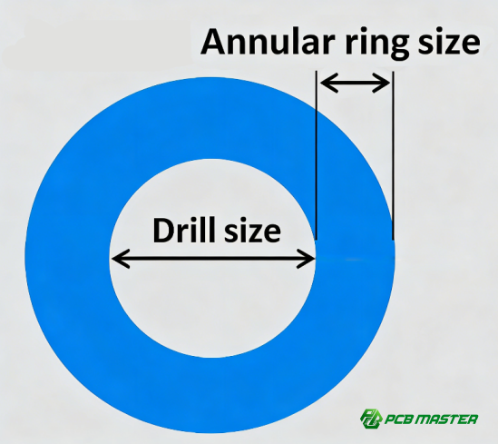
An annular ring refers to a copper ring that surrounds a hole in a printed circuit board (PCB). It is a crucial part of the PCB design process, ensuring reliable electrical and mechanical connections between different layers of the board. The annular ring's primary role is to allow electrical signals to pass through the hole and connect layers of the PCB, while also helping to anchor the hole firmly to the board, preventing separation during manufacturing or operation.
The annular ring consists of three main components:
1. Drilled Hole
This is the physical hole that is drilled into the PCB, which allows components, such as vias, to be placed or connected. The hole serves as a pathway for electrical signals to travel between layers.
2. Copper Plating on the Hole Walls
The drilled hole is then coated with a thin layer of copper, which is chemically deposited. This copper layer connects the hole to the copper circuitry of the PCB layers. The plating ensures that the hole functions as an electrical conduit.
3. Solder Pad (Annular Ring)
Surrounding the hole is a copper ring, which is the solder pad. This pad is found on the PCB's surface and provides a solid anchor for soldering components like vias or other electronic parts. The size of the solder pad is critical in ensuring that the hole can support the component properly, even under mechanical stress.
What is the Role of an Annular Ring?
The role of an annular ring is to provide a mechanical anchor and ensure reliable electrical connections between the layers of a PCB by surrounding the drilled hole with a copper ring.
Providing a Mechanical Anchor Point
The primary function of an annular ring is to act as a mechanical anchor that securely connects the hole in the PCB to the layers of copper. This copper ring surrounds the hole and provides a sturdy bond that helps to prevent the copper plating inside the hole from separating from the PCB layers. Without this mechanical anchor, the hole might detach under stress, such as during manufacturing or when exposed to temperature fluctuations. This anchor ensures that the hole remains securely attached to the PCB, maintaining the integrity of the entire board.
For example, in multi-layer PCBs, where there are several copper layers, the annular ring ensures that signals and power connections remain intact and stable across these layers. This connection is especially critical in applications where high-performance or long-term durability is required, such as in smartphones or medical devices.
Ensuring Electrical Connection Reliability
Another key role of the annular ring is ensuring electrical connection reliability. The ring helps create a stable, continuous path for electrical signals to travel between different layers of the PCB. It ensures that the copper plating inside the hole is connected securely to the copper layers on the PCB’s surface, enabling reliable signal transmission.
Moreover, the annular ring provides a tolerance space to account for any slight misalignment during drilling. When drilling holes in PCBs, small deviations in positioning can occur. The annular ring allows for a margin of error, ensuring that even if the hole is slightly off-center, the electrical connection can still be made. This tolerance space is especially important in high-density PCBs, where precision is critical but small drilling errors can happen.
For example, in a complex PCB design with multiple layers and narrow traces, a small misalignment in drilling could cause a short circuit or prevent proper electrical connections. The annular ring helps avoid such issues by offering extra room for adjustment and ensuring reliable connectivity across layers.
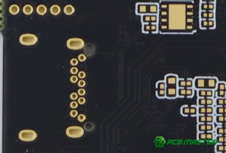
What is a "No-Annular Ring" Hole?
A No-Annular Ring (No-AR) hole is a type of via in a PCB design where the typical copper ring (the annular ring) around the drilled hole is intentionally removed or omitted in certain layers. Unlike traditional vias, which feature a copper ring around the hole to create strong electrical and mechanical connections between layers, No-AR holes skip this step to allow for more flexible routing of signals and components.
This design choice is typically used in high-density interconnect (HDI) PCBs, where space is limited and maximizing the number of connections is essential. By removing the annular ring, more area is available for routing signals, which is especially important in applications like BGA (Ball Grid Array) packages and high-speed circuits where space optimization is crucial.
Characteristics of No-Annular Ring Holes
1. Reduced Copper Area
In a No-AR hole, there is no copper ring around the hole, which reduces the overall copper area on the board. This feature allows for tighter component placement and more room for traces, improving PCB density.
2. Optimized Routing Space
Without the copper ring, the space that would typically be occupied by the annular ring becomes available for routing signals. This makes it easier to route fine traces between closely spaced components, a common requirement in advanced PCB designs.
3. Increased Flexibility in Layout Design
No-AR holes provide greater flexibility for engineers designing PCBs with complex routing requirements. They allow for the placement of vias closer to other components, optimizing the layout without sacrificing electrical connectivity.
4. Targeted Use in Specific Applications
While useful, No-AR holes are typically used only when necessary. They are especially useful in high-density designs, miniaturized electronics, and high-speed circuits, where maximizing available board space is essential.
Why is it Necessary to Design "No-Annular Ring" Holes?
Designing No-Annular Ring holes is necessary to optimize space for routing in high-density PCBs, improve signal integrity, and prevent short-circuit risks, especially in tight areas like BGA components.
BGA Routing Challenges
BGA (Ball Grid Array) components are widely used in high-density PCBs because of their compact design. However, they come with a major challenge—tight pin spacing. In fine-pitch BGA designs, the pins are very close together, which limits the available space for routing electrical signals underneath the component. The traditional annular ring around a via takes up valuable space, making it harder to route traces without running into other components or vias.
By using No-Annular Ring holes, PCB designers can eliminate the copper ring around the hole, freeing up space underneath the BGA component. This allows for more routing options and ensures that signal traces can be routed more efficiently, even in tight spaces. For example, in high-speed communication systems where real estate is limited, this design technique ensures that all connections are made while maximizing available space for the most critical components.
Routing Channel Blockage
Traditional vias with annular rings can obstruct the path of signal traces, especially in areas where space is already tight. The copper ring around a via can block the direct route for traces, making it harder to create an optimized and efficient layout. This is particularly problematic when trying to route signals in high-density designs where space utilization is crucial.
Removing the annular ring allows signal traces to pass closer to the via hole, providing more flexible routing. This leads to better signal integrity and more efficient use of the board area, especially in complex PCB layouts where maximizing every inch is necessary.
Avoiding Short-Circuit Issues
In certain PCB designs, especially those with components that have metallic enclosures or exposed pins, there is a risk of the metal parts coming into contact with the annular ring around a via. This contact can lead to unintended electrical shorts, which can cause the circuit to malfunction or even fail completely.
By designing No-Annular Ring holes, the risk of these short-circuits is reduced. Since there is no copper ring, there is no exposed copper around the hole that could potentially touch metal parts of the components, avoiding the risk of shorts. This feature is particularly important in high-reliability applications, such as medical devices or aerospace electronics, where failure due to shorts can have serious consequences.
How to Implement "No-Annular Ring" PTH Hole Design?
No-Annular Ring PTH hole design can be implemented by directly removing the solder pad in specific layers, using BGA pads with resin plugging, or employing back drilling to remove excess copper from the via.
Direct No-Annular Ring Design
The most straightforward way to design a No-Annular Ring (No-AR) hole is by directly removing the solder pad (the copper ring) around the via in specific layers. This approach is typically applied to the layers where the via does not need to make electrical contact. By eliminating the copper ring, more space is freed up for routing traces, especially in high-density designs where every inch counts.
This method works well when the via’s primary role is just to pass signals between layers, and the surrounding copper ring is not required for the electrical connection. For example, in some high-speed PCB designs where space beneath components like BGAs is limited, removing the annular ring can help with routing without sacrificing signal integrity.
BGA Pad + Resin Plugging
Another method for achieving a No-Annular Ring design is by using the BGA pad itself as the annular ring. In this approach, a via is placed directly in the center of the BGA pad, which serves as the “ring” around the hole. After the via is drilled, resin plugging is used to fill the hole and make it level with the surface of the PCB. This process prevents solder from leaking into the via during the assembly process and ensures the via remains electrically isolated.
This method is particularly useful in BGA designs, where the via is placed under the BGA component and the copper ring would otherwise interfere with the tight spacing. The resin-plugged vias ensure that the vias function without requiring traditional annular rings, optimizing board space.
Back Drilling
Back drilling is another technique used to implement No-Annular Ring holes. In this method, after the via is drilled and copper plating is applied, a larger drill bit is used to remove the extra copper along the inner walls of the via, eliminating the unnecessary annular ring. The process is typically used for high-speed circuits, where signal integrity is critical. By removing the excess copper, the signal paths are cleaner, reducing parasitic capacitance and improving overall signal performance.
Back drilling is often used in multilayer PCBs where vias connect different layers but the copper ring on certain layers is not necessary. The additional drilling removes the unwanted copper, creating a "clean" via that improves signal quality and reduces noise, making it ideal for high-speed signal transmission.
What Are the Benefits of No-Annular Ring PTH Hole Design?
The benefits of No-Annular Ring PTH hole design include increased routing density, improved signal integrity by reducing parasitic capacitance and signal reflections, and more space for efficient inner-layer routing, making it ideal for high-performance and compact PCBs.
Increased Routing Density
One of the primary benefits of No-Annular Ring (No-AR) PTH hole design is its ability to increase the routing density of a PCB. By eliminating the copper ring around the via, more space becomes available for routing traces, which is especially useful in High-Density Interconnect (HDI) designs. In HDI PCBs, the goal is to place more components in a smaller area without compromising performance. No-AR holes allow for tighter placement of vias and traces, making it easier to pack more functionality into a smaller space. This is essential for compact devices like smartphones, wearables, and high-performance computing systems.
For example, in advanced consumer electronics, where miniaturization is key, No-AR hole design enables engineers to fit more layers and connections within a limited PCB footprint, improving the overall design and functionality.
Improved Signal Integrity
Removing the annular ring also improves signal integrity, particularly for high-speed signals. The copper ring around a via can create unwanted parasitic capacitance—a type of electrical interference that can slow down signal transmission or distort the signal. By eliminating the ring, the capacitance is reduced, allowing for faster, cleaner signal flow.
Additionally, back drilling (removing excess copper from the via) can further improve signal integrity by reducing signal reflections and attenuation (weakening of the signal). In high-speed circuits, this is crucial for maintaining signal quality, reducing noise, and preventing errors. For instance, in high-frequency communication systems or digital circuits, reducing capacitance and reflections leads to better performance and fewer signal losses.
More Space for Inner Layer Routing
No-AR hole design frees up valuable space, allowing designers to route traces more effectively, especially on inner layers of a multilayer PCB. By removing the annular ring, designers can create more efficient layouts and route more signals within a limited number of layers. This helps in achieving complex routing within a constrained board, particularly when the PCB needs to handle numerous connections in a compact form.
In practical terms, this is especially beneficial when designing for multilayer boards where engineers need to maximize the available area. For example, in automotive applications, where the PCB needs to fit into a small control unit while managing a complex network of sensors and actuators, No-AR hole design makes it possible to achieve the required complexity without increasing board size.
What Challenges and Drawbacks Are Associated with No-Annular Ring PTH Hole Design?
The challenges and drawbacks of No-Annular Ring PTH hole design include reduced reliability due to weaker connections, high precision manufacturing requirements, increased costs, and difficulties in testing and maintenance.
Reliability Risks
One of the major challenges of No-Annular Ring (No-AR) PTH hole design is the reduced reliability due to the lack of a solder pad (the copper ring). The annular ring typically serves as a mechanical anchor that ensures a strong connection between the copper plating inside the hole and the layers of the PCB. Without this anchoring, the copper layer inside the hole may have a weaker bond to the PCB layers. This makes the hole more vulnerable to thermal stress and mechanical stress that can occur during manufacturing or during the life of the device. In applications where PCBs are exposed to high temperatures or mechanical movements, the risk of the via breaking free from the layers or cracking increases. For instance, in automotive electronics, where high heat and vibration are common, this lack of mechanical stability could lead to premature failure.
High Manufacturing Precision Requirements
No-AR PTH holes require high precision in both alignment and drilling to ensure the via connects properly across the layers. The removal of the copper ring leaves no margin for error, and even slight misalignments can result in the failure of the electrical connection between layers. This requires high-precision equipment to drill the vias and align the layers accurately during manufacturing. Additionally, the plating process for the via needs to be highly uniform and strong, as the lack of an annular ring means there is less surface area for the copper plating to bond with. Manufacturing with high precision and ensuring that the via meets the required strength and uniformity can be challenging, especially in complex designs or with larger PCBs that require multiple layers.
Increased Costs
Due to the specialized equipment, high precision, and advanced manufacturing techniques required, No-Annular Ring PTH hole design increases the overall cost of PCB production. The use of advanced drilling machines, improved alignment systems, and enhanced plating processes to ensure uniformity and strength all contribute to higher manufacturing costs. Additionally, quality control becomes more complex, requiring more advanced testing methods to ensure the vias are properly formed and meet specifications. This makes No-AR PTH holes more expensive compared to traditional designs with annular rings. For companies that need to keep costs low, such as in consumer electronics, this may not be a cost-effective solution.
Difficulties in Testing and Maintenance
The absence of the annular ring around the hole also creates difficulties in testing and maintenance. Traditional optical inspection methods, like Automated Optical Inspection (AOI), are often used to check vias for proper connections. However, No-AR holes make it harder for these systems to detect issues, as there is no visible copper ring to examine. Without an easily identifiable copper ring, it is more difficult to verify that the via is properly connected, making the process of quality control more complex. Furthermore, if a fault occurs in the PCB, diagnosing and repairing it is much more challenging because there is less visual information to work with. For example, if a via breaks free from its connection due to thermal stress, the failure may not be immediately visible, making repair efforts more time-consuming and costly.
Applications of No-Annular Ring PTH Design
No-Annular Ring PTH design is widely used in communication systems and consumer electronics to enable miniaturization, enhance routing density, and ensure high-performance in compact devices like smartphones, 5G systems, and gaming consoles.
In Communication Systems
No-Annular Ring (No-AR) PTH design plays a significant role in the communication industry, particularly in devices that require both miniaturization and high performance. Communication devices like smartphones, tablets, and routers need to be compact but also capable of handling complex circuitry and fast data transmission. No-AR holes are ideal for such applications because they allow for higher routing density, which makes it possible to place more components in a smaller area. This helps meet the demand for compact devices without compromising on performance.
For example, in 5G communication systems, where high-frequency signals and complex PCBs are involved, No-AR holes reduce parasitic capacitance and ensure signal integrity while saving valuable space on the PCB. By removing the copper ring, engineers can achieve high-speed signal transmission in a smaller form factor, making it perfect for mobile communication technology, IoT devices, and other compact communication products.
In Computing and Consumer Electronics
The demand for high-density PCBs is especially important in the computing and consumer electronics industries, where devices like laptops, gaming consoles, and wearable tech are becoming increasingly smaller yet more powerful. These products require efficient use of PCB real estate to fit advanced components while maintaining high performance and low latency.
No-AR PTH designs allow for the miniaturization of these devices by enabling more compact, higher-density routing within the PCB. The reduced need for large copper rings frees up space for more signal traces and component placement, improving overall device performance and allowing for the inclusion of advanced technologies like multi-layer boards and HDI designs. This is critical in consumer products like smartwatches or ultra-thin laptops, where every millimeter of space matters.
In the gaming industry, for instance, high-performance graphics and processors require precise, fast signal transmission between layers of the PCB, making No-AR hole designs a valuable tool for enhancing the performance of compact gaming consoles or gaming laptops without compromising on connectivity.
Conclusion
No-Annular Ring PTH designs are essential for achieving high-density, high-performance PCBs, especially in compact and advanced devices across various industries like communication and consumer electronics. However, implementing this design requires precision and expertise to ensure reliability and performance.
For those seeking reliable and high-quality No-Annular Ring PTH designs, PCBMASTER, a seasoned PCB and PCBA supplier, offers tailored solutions to meet specific needs. With years of experience, PCBMASTER is committed to delivering top-notch products that ensure the best in functionality and design, helping businesses bring their innovative electronics to life with precision and efficiency.
FAQs
When is "No-Annular Ring" PTH Design Required?
No-Annular Ring PTH design is typically used in high-density interconnect (HDI) PCB designs, where space is at a premium and high-performance functionality is required. This design is especially beneficial in applications like BGA (Ball Grid Array) packages, where the space between the pads is very limited, and high-speed signal transmission, such as in 5G communication systems, advanced computing devices, and wearable electronics, where maintaining signal integrity is critical. In these cases, the removal of the copper ring around the via enables designers to place more traces in the same area, maximizing the use of available space while ensuring minimal signal interference.
What Are the Main Risks of No-Annular Ring PTH Hole Design?
The primary risk associated with No-Annular Ring PTH design is the potential weakening of the via's mechanical bond with the PCB layers. The absence of the copper ring reduces the surface area available for adhesion between the via's inner copper plating and the surrounding layers of the PCB. This weakened bond makes the via more vulnerable to thermal and mechanical stresses. During processes like soldering, or under temperature fluctuations during the PCB’s operational life, the connection could weaken or crack, leading to potential failure of the electrical connection between layers. This is a significant risk in high-reliability applications, such as automotive or aerospace electronics, where the PCB is subjected to high temperatures or vibration.
How Does No-Annular Ring PTH Design Affect Signal Integrity?
No-Annular Ring PTH design can significantly improve signal integrity by reducing parasitic capacitance. Parasitic capacitance arises when the copper ring around a via forms an unwanted capacitor between the layers of the PCB. This capacitance can distort high-speed signals, especially in high-frequency applications. By removing the copper ring, the signal path is cleaner, with less interference or loss of signal quality. Furthermore, removing the annular ring ensures that signal traces can be routed closer to the via without encountering copper pads that could affect the signal, improving overall signal transmission quality. This is particularly valuable in designs requiring high-speed data transfer, such as high-frequency RF circuits or digital communication.
How to Ensure Manufacturing Accuracy for No-Annular Ring PTH Designs?
To ensure the reliability and performance of No-Annular Ring PTH designs, manufacturers need to achieve high precision in several areas:
l Layer Alignment: The alignment between different layers of the PCB is critical to ensure that the vias connect correctly across layers. Any misalignment can result in open circuits or short circuits.
l Drilling Precision: The drilling process must be extremely accurate to create vias that meet the required specifications. Any variation in the hole's diameter or positioning can result in poor electrical connections or mechanical integrity issues.
l Electroplating: The electroplating process used to apply copper to the vias must ensure uniformity in the thickness of the copper plating. This is essential to guarantee that the via has the necessary mechanical strength to withstand thermal stresses and maintain a reliable connection. Manufacturers often rely on specialized equipment to maintain these high precision standards.
Is No-Annular Ring PTH Design More Expensive Than Traditional Designs?
Yes, No-Annular Ring PTH designs are typically more expensive than traditional designs for several reasons:
l Higher Manufacturing Precision: To create a No-Annular Ring hole, manufacturers need to use high-precision equipment, such as laser drilling and advanced alignment systems, which significantly increases the cost compared to standard designs with an annular ring.
l Advanced Plating and Inspection: The plating process for No-Annular Ring holes requires more careful control to ensure the copper adhesion strength is adequate, and extra inspection steps are needed to confirm the via’s integrity, further raising costs.
l Increased Design Complexity: No-Annular Ring PTH designs often require more intricate design and testing, which can increase the overall cost of the PCB development process.
Overall, while No-Annular Ring PTH designs offer advantages like higher routing density and improved signal integrity, they come at a higher cost due to the specialized equipment, precision, and quality control required. For many high-performance and compact applications, however, the benefits justify the added expense.
Author Bio
Hi, I'm Carol, the Overseas Marketing Manager at PCBMASTER, where I focus on expanding international markets and researching PCB and PCBA solutions. Since 2020, I've been deeply involved in helping our company collaborate with global clients, addressing their technical and production needs in the PCB and PCBA sectors. Over these years, I've gained extensive experience and developed a deeper understanding of industry trends, challenges, and technological innovations.
Outside of work, I'm passionate about writing and enjoy sharing industry insights, market developments, and practical tips through my blog. I hope my posts can help you better understand the PCB and PCBA industries and maybe even offer some valuable takeaways. Of course, if you have any thoughts or questions, feel free to leave a comment below—I'd love to hear from you and discuss further!

