


Advanced HDI PCB Manufacturing: Key Technologies Shaping Future Electronics
Driven by the explosive growth of AI computing, 5G/6G communications, autonomous vehicles, and high-performance electronics, HDI PCB technology is evolving rapidly toward ultra-high density, faster signal transmission, and greater reliability. Advanced manufacturing processes such as mSAP, ultra-fine laser microvias, high-speed low-loss materials, and intelligent inspection systems are reshaping the future of PCB production.
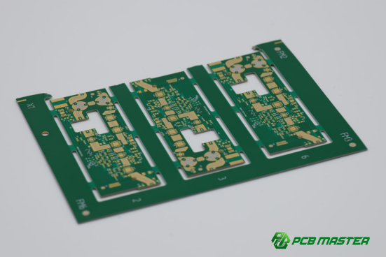
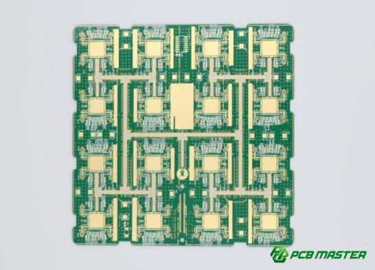
Modern PCB manufacturing is no longer limited to basic electrical interconnection. Instead, it is becoming a critical foundation for intelligent electronic systems that require superior signal integrity, thermal management, miniaturization, and long-term reliability. As a professional PCB and PCBA manufacturer, PCBMASTER leverages advanced HDI capabilities, high-frequency materials, rapid prototyping, and strict quality control systems to support next-generation applications across AI servers, automotive electronics, telecommunications, industrial control, and high-speed computing markets.
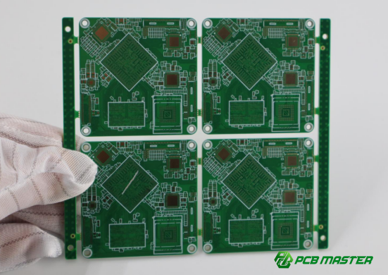
Ultra-Fine HDI Structures and Higher-Order Interconnections
The Evolution of Microvias and Fine-Line Technology
HDI PCB technology is rapidly advancing toward ultra-fine circuitry and higher interconnection density. Current mass production capabilities have reached laser microvias below 50μm and 30μm/30μm line width and spacing, while leading manufacturers are developing 25μm microvias and 15μm/15μm ultra-fine circuits for next-generation electronics.
These ultra-dense structures are essential for AI chips, HPC servers, advanced packaging substrates, and high-speed communication equipment, where signal integrity, miniaturization, and routing efficiency are critical.
mSAP Technology Becoming the Industry Standard
Modified Semi-Additive Process (mSAP) is becoming the core manufacturing technology for advanced HDI PCBs. Compared with traditional subtractive etching, mSAP enables much finer circuit formation with higher precision, lower signal loss, and improved copper uniformity.
The process relies on ultra-thin copper foil, LDI laser direct imaging , and precision electroplating to achieve extremely fine patterns and stable electrical performance, especially for high-frequency and high-speed applications.
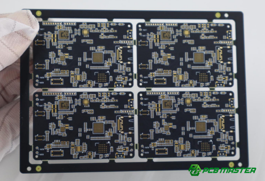
Advanced Stacking Technologies
The industry is also moving beyond conventional Any-layer HDI structures toward more advanced interconnection architectures such as ELIC (Every Layer Interconnection) . Third-order and fourth-order HDI designs are increasingly used in AI servers, high-speed switches, and advanced semiconductor packaging.
To improve long-term reliability, staggered microvia stacking is widely adopted to reduce stress concentration and enhance thermal and mechanical stability.
| Dimension | Conventional PCB | Advanced HDI PCB / PCBMASTER Capability |
| Via Size | Larger mechanical vias | Ultra-fine laser microvias |
| Circuit Density | Moderate | Ultra-high density |
| Signal Integrity | Standard | Optimized for high-speed transmission |
| Applications | Consumer electronics | AI, 5G, automotive, servers |
| Reliability | Conventional | Enhanced thermal and mechanical reliability |
Advanced Materials Driving Next-Generation PCB Performance
Ultra-Low-Loss Materials for High-Speed Applications
As data rates escalate toward 112Gbps and 800G optical transmission systems, PCB materials must deliver extremely low dielectric loss and stable signal integrity. Traditional FR-4 materials are no longer sufficient for these high-frequency environments.
Advanced solutions such as PTFE composites, modified polyimide materials, and low-roughness copper foils are increasingly used to reduce signal attenuation and improve high-speed performance. These materials play a critical role in optimizing dielectric properties and ensuring stable transmission in AI servers, high-speed switches, and communication infrastructure.
Thermal Management Materials for AI and High-Power Devices
The rapid growth of GPUs , CPUs , and AI accelerators has created severe thermal challenges in modern PCB design. Efficient heat dissipation is now a core requirement rather than an optional feature.
To address this, advanced thermal solutions such as embedded thermal blocks, metal-core PCB structures, and high thermal conductivity prepregs are widely adopted. These technologies help distribute and dissipate heat effectively, improving system stability and extending device lifespan in high-power applications.
High-Reliability and Eco-Friendly Materials
Reliability is especially critical in automotive and industrial electronics, where long-term stability and harsh operating environments are standard requirements. High Tg materials are used to maintain structural integrity under elevated temperatures, while enhanced CAF resistance improves long-term electrical reliability.
In addition, halogen-free and phosphorus-free flame retardant materials are increasingly adopted to meet environmental regulations and global sustainability standards. These material advancements ensure that next-generation PCBs are not only high-performing but also compliant with international safety and environmental requirements.
Advanced PCB Manufacturing Processes Reshaping the Industry
Ultra-Fine Circuit Manufacturing
The transition from traditional subtractive etching to mSAP (Modified Semi-Additive Process) is a key milestone in modern PCB manufacturing. This shift enables significantly finer circuitry, improved dimensional control, and better electrical performance for high-speed applications.
Critical process controls in advanced manufacturing include sub-2μm copper deposition, LDI precision below 10μm, high-stability electroplating, and strict side-etch control. These parameters are essential for achieving ultra-fine line structures required in HDI and high-frequency PCB designs.
Roll-to-Roll (R2R) Manufacturing for Flexible Electronics
Roll-to-roll manufacturing is increasingly used in FPC and rigid-flex PCB production. This approach improves production efficiency while supporting large-scale, continuous fabrication of flexible circuits.
It is particularly valuable for wearable devices, compact consumer electronics, and space-constrained applications where flexibility, light weight, and high integration are required.
Laser Drilling and Precision Processing Technologies
Advanced PCB manufacturing relies heavily on ultrafast pulse laser technology to create precise microvias with minimal thermal damage. Compared to mechanical drilling, laser processing offers cleaner hole walls, reduced thermal impact zones, and higher accuracy.
CO₂ and UV laser hybrid systems are used to optimize processing across different material layers, while laser direct opening (LDO) technology enables precise coverlay window formation in flexible circuits.
Advanced Electroplating and Embedded Technologies
Modern PCB fabrication increasingly uses pulse plating and horizontal plating techniques to ensure uniform copper distribution in high-aspect-ratio structures. Selective electroless and electroplating processes further enhance precision in localized reinforcement areas.
Embedded technologies such as copper blocks, resistors, and capacitors are also gaining traction, enabling higher integration density and improved electrical performance while reducing board size.
Manufacturing Innovation Comparison
| Technology | Traditional Process | Frontier Manufacturing Approach |
| Imaging | Film exposure | LDI direct imaging |
| Drilling | Mechanical drilling | Ultrafast laser drilling |
| Circuit Formation | Subtractive etching | mSAP process |
| Plating | Conventional plating | Pulse/horizontal plating |
| Reliability | Standard QC | Intelligent precision control |
Inspection, Testing, and Reliability Assurance in Advanced PCBs
High-Precision Inspection Technologies
As PCB structures become increasingly dense and complex, advanced inspection technologies are essential to ensure manufacturing quality and defect-free performance. Automated X-ray inspection (AXI) is widely used to detect hidden solder joint issues and internal structural defects that are not visible through conventional optical methods.
In addition, 3D X-ray CT scanning provides full volumetric analysis of multilayer HDI structures, enabling precise evaluation of embedded components, via integrity, and internal interconnection quality. These technologies significantly improve defect detection accuracy and manufacturing reliability in high-end PCB applications.
Electrical and Reliability Testing
Modern PCB validation requires a combination of electrical and environmental stress testing. Flying probe testing and boundary scan testing are used to verify electrical continuity and functional performance in high-density interconnections.
Reliability testing includes CAF (Conductive Anodic Filament) testing, thermal cycling, high-temperature/high-humidity exposure, and mechanical drop and impact testing. These processes simulate real-world operating conditions to ensure long-term stability and durability in demanding applications.
Why Reliability Is Critical for Future Electronics
Reliability has become a core requirement in modern electronics due to the increasing use of PCBs in safety-critical and high-performance systems. Automotive electronics demand strict safety compliance, AI servers require continuous uptime, and industrial control systems depend on stable long-term operation.
PCBMASTER’s Quality Assurance Approach
As a professional PCB and PCBA manufacturer, PCBMASTER implements a comprehensive quality assurance system aligned with ISO 9001 and IATF 16949 standards. Its manufacturing processes are also UL and RoHS certified, ensuring global compliance and environmental safety.
Quality control is reinforced through advanced AOI inspection, a three-stage inspection system, and strict process monitoring. With a 99.5% product yield rate and 99.59% on-time delivery capability, PCBMASTER ensures consistent reliability and performance across complex HDI and high-frequency PCB applications.
Emerging Substrate Technologies and the Future of PCB Innovation
Glass Substrates: The Next Generation of High-Speed Interconnection
Glass substrates are emerging as a promising solution for next-generation high-speed and high-density interconnection systems. Compared with traditional organic laminates, glass offers significantly improved dimensional stability, enabling tighter feature scaling and more precise multilayer alignment.
Key advantages include superior high-frequency performance, excellent flatness control, and the potential for large-panel manufacturing, which can improve production efficiency and cost scalability. These characteristics make glass substrates particularly attractive for advanced semiconductor packaging, AI computing platforms, and next-generation communication systems. As a result, major semiconductor companies are increasingly investing in glass substrate research and development.
Ceramic Substrates in Extreme Applications
Ceramic substrates continue to play a critical role in applications requiring extreme thermal, electrical, and environmental performance. They are widely used in high-power systems, millimeter-wave communications, aerospace electronics, and defense-grade devices.
Their inherent stability under high temperatures and harsh operating conditions makes them ideal for mission-critical systems. In advanced designs, ceramic substrates are increasingly integrated with HDI PCB technologies to combine high-density interconnection with exceptional reliability and performance.
These emerging substrate technologies are redefining the boundaries of PCB innovation, enabling the development of more powerful, compact, and reliable electronic systems for future applications.
Practical Industry Challenges and Engineering Considerations
Common Design Mistakes in Advanced HDI Projects
As HDI PCB designs become more complex, engineering errors have a greater impact on yield, performance, and reliability. One of the most common issues is improper stack-up design, which can lead to impedance mismatch, routing inefficiencies, and manufacturing constraints.
Thermal management neglect is another critical problem, especially in high-power applications such as AI accelerators and automotive control units. Poor heat distribution can significantly reduce device lifespan and stability. In addition, signal integrity issues often arise in high-speed designs when return paths, spacing rules, or material properties are not properly considered.
Finally, inadequate Design for Manufacturability (DFM) review frequently results in unnecessary redesign cycles, increased cost, and delayed product launches.
How Early Engineering Collaboration Reduces Risks
Early-stage collaboration between designers and manufacturers is essential for reducing project risks and optimizing overall performance. Free engineering document review allows potential manufacturability issues to be identified before production begins.
This process improves design efficiency through stack-up optimization, cost reduction strategies, and early identification of high-risk features. As a result, product development cycles become faster and more predictable, especially in high-complexity HDI and rigid-flex projects.
PCBMASTER’s Engineering Support Advantages
As a professional PCB and PCBA manufacturer, PCBMASTER provides a comprehensive engineering support system integrated with advanced HDI manufacturing capabilities.
Key advantages include 24-hour rapid prototyping, one-on-one engineering consultation, and a transparent online quotation system. The company also supports flexible PCB, rigid-flex PCB, and complex multilayer customization, backed by an 80,000㎡ self-owned manufacturing facility and global logistics capability.
A typical application scenario is in AI, automotive, and communication hardware development, where early engineering support and rapid-turn manufacturing significantly reduce iteration cycles, improve design accuracy, and accelerate time-to-market for complex electronic systems.
Future Trends: From Interconnection Platforms to Intelligent Electronic Foundations
The Three Core Drivers of Future PCB Innovation
The evolution of PCB technology is being shaped by three fundamental forces that are redefining design complexity and manufacturing capability. First, advanced semiconductor packaging is demanding far higher interconnection density and electrical performance than traditional PCB architectures can support.
Second, the rapid expansion of AI, 5G/6G communications, and high-speed computing is pushing signal transmission speeds and bandwidth requirements to new extremes, requiring ultra-low-loss materials and precision manufacturing. Third, continuous miniaturization in consumer electronics and the increasing safety-critical nature of automotive systems are driving stricter reliability and integration requirements.
The Future Direction of HDI PCB Technology
HDI PCB technology is moving toward a more integrated and intelligent future characterized by higher circuit density, faster signal transmission, and significantly improved thermal management capabilities. At the same time, reliability systems are becoming more advanced, incorporating predictive quality control and multi-layer validation mechanisms.
A key trend is the deeper integration of PCB structures with semiconductor packaging technologies, enabling more compact system-in-package (SiP) and advanced module-level designs that bridge the gap between chip and system-level performance.
Final Thoughts
The future of PCB development is defined by the convergence of extreme density, high-speed signal integrity, intelligent manufacturing processes, and advanced reliability engineering. These factors collectively transform PCBs from simple interconnection substrates into intelligent electronic foundations for next-generation systems.
Manufacturers capable of mastering these frontier technologies — such as PCBMASTER — will play a critical role in enabling innovation across AI hardware, telecommunications, automotive electronics, and high-performance computing industries.
Tags
#HDIPCB #PCBManufacturing #PCBA #SMT #HighSpeedPCB #RigidFlexPCB #AIHardware #5G #6G #AutomotiveElectronics #PCBMASTER #ElectronicsManufacturing #AdvancedPCB #IndustryInsights
About the Author

Carol Luo
PCB Design EngineerI'm Carol, a PCB Engineer at PCBMASTER with experience in PCB design and manufacturing engineering since 2018. I focus on translating engineering requirements into reliable PCB solutions, with expertise in stack-up design, material selection, and design-for-manufacturing (DFM). I share practical engineering insights from real-world PCB design and production experience.
Visit Carol Luo's Profile
