


The Benefits of Copper Based Superconductors PCB in Modern Electronics
Introduction
When electric current can flow through circuits without any resistance, when energy transmission no longer generates heat loss—what kind of transformation will the world of electronic devices undergo? This is quietly becoming a reality with the development of copper-based superconducting PCB technology.
In today's rapidly evolving electronics industry, traditional printed circuit boards (PCBs) are facing unprecedented challenges. With the advancement of technologies like 5G, artificial intelligence, high-performance computing, and electric vehicles, demands on the current-carrying capacity, heat dissipation, and energy efficiency of circuit boards are higher than ever.
A novel solution merging superconducting materials with PCB technology—copper-based superconducting PCBs—is moving from the laboratory towards industrialization, poised to fundamentally change how we design and use electronic devices.
Copper-Based Superconducting PCBs: Upending the Foundations of Conventional Electronics

Traditional PCBs use copper as a conductive material, but its resistivity increases sharply as dimensions shrink, leading to growing problems of energy consumption and heat generation. In the miniaturization of chip interconnects, when line widths drop below 10 nanometers, the resistance of copper increases drastically, adversely affecting overall circuit performance.
Traditional PCBs often use a copper core or copper substrate as the core material to enhance thermal and electrical performance.
The structure of PCBs typically includes a circuit layer and a conductive layer, which are essential for forming electrical pathways and supporting heat dissipation.
Copper-based superconducting PCBs, which are an evolution of copper core PCBs, perfectly solve this problem by achieving zero-resistance conductivity under specific low-temperature conditions. This technology does not simply use copper as a conductor but involves creating special copper-based composite materials that exhibit superconducting properties under specific conditions.
In 2018, researchers at the National Institute of Standards and Technology (NIST) discovered a novel plated metal combination—an ultrathin rhenium layer sandwiched between gold layers—that could achieve superconductivity at relatively attainable temperatures. This material combination has a superconducting critical temperature above 6 Kelvin. While still requiring a cryogenic environment, this discovery opened new possibilities for applying superconducting materials in circuit boards.
The Miracle Material: How Copper-Based Superconductors Work
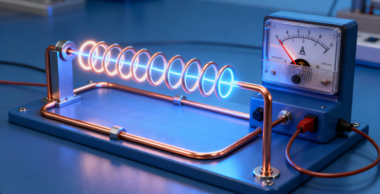
The phenomenon of superconductivity was first discovered by Dutch physicist Heike Kamerlingh Onnes in 1911. When certain materials are cooled below a specific critical temperature, their electrical resistance abruptly drops to zero. To achieve this state, superconducting materials must be maintained at an appropriate temperature, which often involves managing both high and low temperatures to ensure zero resistance. Conventional superconductors required operation at extremely low temperatures near absolute zero, severely limiting their practical application.
The discovery of copper-based high-temperature superconductors changed this landscape. These materials can achieve superconductivity at significantly higher temperatures, some even operating above liquid nitrogen temperatures (77 K), substantially reducing cooling costs and complexity. This ability to function at high temperatures makes them suitable for applications exposed to both high and low temperatures, improving durability and performance.
The operating principles of copper-based superconducting PCBs are based on the unique properties of these materials. The structure of these superconductors often includes multiple metal layers and a dielectric layer, which help optimize performance and thermal management at high temperatures.
Zero Resistance Effect
In the superconducting state, current flows through the material without encountering any resistance, meaning almost no energy is lost during transmission.
Perfect Diamagnetism
Superconducting materials expel external magnetic fields. This property can be leveraged to design entirely new circuit architectures and electromagnetic shielding solutions.
Quantum Tunneling Effect
Superconducting electron pairs can tunnel through energy barriers that are normally impenetrable, enabling novel signal processing methods
Transforming the PCB Industry: From Conductive to "Superconductive"
In traditional PCB manufacturing, heavy copper PCBs have already secured their place in high-power applications due to their superior current-carrying capacity. For instance, copper substrates can easily handle large currents of several hundred amperes while efficiently dissipating heat. In addition to heavy copper PCBs, copper core PCBs offer significant advantages such as superior thermal conductivity, high thermal conductivity, and great thermal conductivity, which enable efficient heat transfer and effective management of high temperatures in demanding environments.
Conventional PCB copper foil thickness typically ranges from 1 to 3 ounces, whereas heavy copper PCBs can have copper thicknesses from 3 to 20 ounces or even more. However, when current passes through these traditional copper traces, heat is still generated due to resistive effects, resulting in energy waste and device temperature rise. Metal core PCBs, including copper core PCBs and aluminum-based PCBs, are specifically designed to handle high density and high power applications, providing enhanced durability and improved thermal management.
The emergence of copper-based superconducting PCBs is set to overhaul this scenario completely. In high-density, high-frequency, and high-temperature environments, copper-based PCBs and metal core PCBs are preferred due to their excellent thermal conductivity and ability to dissipate heat generated by electronic components, improving energy efficiency and integration density. The transition from traditional to superconducting PCBs highlights that copper base and copper substrate are foundational elements in the evolution of printed circuit board technology.
In summary, the use of core PCBs, especially those with a metal core, provides significant advantages in terms of heat transfer, durability, and performance, making them ideal for advanced printed circuit board applications.
Revolutionary Improvement in Energy Efficiency
Zero resistance means virtually no energy loss during transmission. For large data centers and server farms, this leap in energy efficiency translates into massive cost savings and reduced carbon emissions. Imagine a processor that generates no heat or a power module with negligible energy loss—this will redefine the energy efficiency standards for electronic devices.
A Quantum Leap in Integration Density
Superconducting traces can withstand higher current densities, allowing for the design of finer line widths and spacing. As technology nodes continue to shrink, local interconnect line widths have already fallen below 10 nanometers. Copper-based superconducting materials can maintain excellent conductive properties even at these scales, enabling integration densities far surpassing those of traditional copper interconnects.
A Fundamental Shift in Thermal Design
In conventional electronic devices, roughly 30-40% of energy is wasted as heat. Superconducting PCBs generate almost no heat, meaning thermal management design can be fundamentally simplified. Devices can be made smaller and more compact without worrying about overheating.
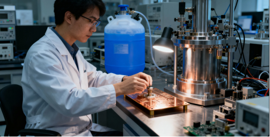
Fabrication Processes: The Manufacturing Challenges of Copper-Based Superconducting PCBs
The manufacturing process for copper-based superconducting PCBs combines traditional PCB techniques with superconducting material preparation methods. During the patterning and etching of copper and aluminum layers, chemicals such as sodium hydroxide and hydrogen peroxide are commonly used as etchants or cleaning agents to achieve precise metal patterning and surface preparation. In the assembly and bonding of layers, pressure is applied during lamination to ensure strong adhesion, and wire bonding is often used in advanced PCB designs to establish reliable electrical connections between components and the circuit.
For surface finishes, silver plating and immersion gold are popular options that improve solderability, enhance durability, and protect the PCB surface. When selecting substrate materials, aluminum and aluminum PCBs are frequently chosen as alternatives to copper for their excellent thermal conductivity, cost-effectiveness, and suitability in high-power applications. Double-sided PCBs, which feature conductive layers on both sides of the metal core, offer increased design flexibility and are used in more complex multilayer structures.
During assembly, solder and advanced soldering techniques are essential for connecting components and protecting the circuit layer from oxidation and environmental damage.
Substrate Selection and Processing
Choosing a suitable substrate material is the crucial first step. Researchers are exploring various techniques for growing superconducting thin films on metal substrates to create superconducting circuit bases with high thermal stability and mechanical strength.
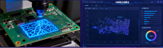
Patterning Superconducting Traces
Similar to traditional PCBs, superconducting circuits need to be patterned into specific layouts. This typically involves:
·Laser Direct Imaging (LDI): High-precision pattern transfer with resolutions reaching 10 micrometers.
·Electrochemical Deposition: Depositing superconducting materials in specific areas.
·Dry Etching: Precisely removing excess material to form the circuit patterns.
Cryogenic Integration
Copper-based superconducting PCBs require a low-temperature environment to operate, necessitating the integration of cooling systems directly into the circuit board design. Advanced micro-refrigeration technologies are being developed to provide compact and efficient temperature control solutions.
Application Prospects: From Consumer Electronics to Quantum Computing
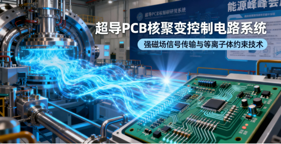
Once mature, copper-based superconducting PCB technology promises revolutionary changes across numerous fields. These PCBs are ideal for protecting critical components in high-power and high-temperature applications, ensuring system reliability and longevity.
In power electronics and energy conversion, copper-based superconducting PCBs are used in power rectifiers, power controllers, and switching regulators to enable efficient power management and conversion in demanding environments.
For communication technology, these PCBs find application in balanced amplifiers and audio equipment, where high fidelity, low noise, and signal integrity are essential for optimal performance.
In lighting, copper-based superconducting PCBs are widely used in LED lighting solutions, such as street lamps, downlights, stage lights, mining lamps, and ship lights, due to their superior thermal management capabilities.
Overall, copper-based superconducting PCBs are more environmentally friendly because of their durability, recyclability, and reduced need for additional cooling hardware, contributing to a lower environmental impact.
High-Performance Computing and Artificial Intelligence
Superconducting computing architectures can perform mathematical operations at ultra-high speeds with extremely low power consumption. For AI applications processing massive datasets, this means exponential performance gains coupled with drastically reduced energy consumption.
Power Electronics and Energy Conversion
In the renewable energy sector, copper-based superconducting PCBs could be used for highly efficient energy conversion and transmission. For example, in photovoltaic inverters, superconducting materials could carry DC currents exceeding 200 A while keeping the junction temperature of power devices low.
Communication Technology
Radio frequency power amplifiers in 5G/6G base stations must handle both high power and high-frequency signals. The low-loss characteristics of copper-based superconducting PCBs could significantly reduce signal distortion, improving communication quality and efficiency.
Quantum Computing
Superconducting circuits are one of the most promising pathways towards realizing quantum computing. Copper-based superconducting PCBs could provide a stable and reliable platform for controlling and reading out qubits, accelerating the progress towards practical quantum computers.
Medical Electronics
Technical Challenges and Future Development Directions
Despite the promising prospects, moving copper-based superconducting PCBs from the lab to industrialization faces several hurdles:
First, the fabrication process for superconducting PCBs is not as mature as that for traditional copper PCBs. Multilayer PCB designs, which can include up to 8 circuit layers, are increasingly used to achieve higher integration and performance, but they add complexity to the manufacturing process.
Second, material selection is critical. While copper is a good conductor and widely used for its excellent electrical properties, superconducting materials offer even lower resistance at low temperatures, which is essential for certain advanced applications.
Temperature Limitations
Most current copper-based superconducting materials still require temperatures below that of liquid nitrogen. While this is a significant improvement over conventional superconductors, cooling costs remain a practical consideration. The search for superconducting materials with higher critical temperatures is a primary focus of future research.
Maturity of Fabrication Processes
The processes for creating superconducting materials are far more complex than those for traditional copper foil, requiring precise control over material composition and crystal structure. For instance, while plated rhenium shows excellent superconducting properties, its process still needs optimization for large-scale manufacturing.
Integration with Existing Technology
Integrating superconducting PCBs with conventional semiconductor devices presents a significant challenge. This demands the development of new interface technologies and packaging processes to ensure seamless collaboration between superconducting and conventional sections.
Cost Considerations
Currently, the production cost of superconducting materials is high. Costs are expected to decrease with process improvements and scaled-up production. Research indicates that the rhenium plating process is "easily scalable for mass production," offering hope for cost reduction.
Future Outlook: A Revolutionary Convergence Point

Copper-based superconducting PCB technology is at a critical juncture, transitioning from laboratory research towards industrialization. With advancements in materials science and fabrication technologies, it is reasonable to believe this technology will gradually become practical within the next 5-10 years.
Companies such as D-Wave Systems and D-Wave Systems Inc. are actively involved in research, patent filings, and commercialization of superconducting technologies, driving innovation and shaping the industry's future.
Future developments will likely follow these directions:
1.Hybrid Structure PCBs: Integrating conventional conductive sections and superconducting sections on the same board, optimized for different requirements.
2.Room-Temperature Superconducting PCBs: Achieving superconductivity at room temperature would utterly transform the entire electronics industry. While still in the realm of scientific aspiration, the discovery of new materials and mechanisms continually pushes this goal closer.
3.Multi-Dimensional Superconducting Circuits: Leveraging the unique quantum properties of superconducting materials to develop new computing architectures that rely not just on the two-dimensional flow of current but potentially on three-dimensional quantum states.
4.Self-Powered Superconducting Systems: Combining superconducting energy storage with highly efficient energy transmission to create autonomous electronic systems requiring minimal external power.
Conclusion
Copper-based superconducting PCB technology represents a significant future direction for the electronics industry. It is not merely an innovation in materials but a revolution in the entire architecture and design philosophy of electronic devices. As research deepens and the technology matures, we can anticipate a new era of electronic devices characterized by extremely high energy efficiency, supercomputing capabilities, and unprecedented levels of integration.
For PCB industry professionals, electronics engineers, and technology investors, now is the prime time to focus on and potentially invest in this cutting-edge technology. Seizing the pulse of material transformation is key to gaining a leading position in the next wave of industrial upgrading.
The significance of this revolution extends beyond mere technical performance enhancements; it has the potential to reshape the entire technological roadmap and ecosystem of the electronics industry. From energy conservation to quantum leaps in computing power, copper-based superconducting PCB technology is sketching the blueprint for a more efficient and powerful electronic future.
FAQs
Q. What is a superconducting copper-based PCB?
A. A superconducting copper-based PCB is a printed circuit board that uses copper as its base material and possesses superconducting properties. It can achieve zero-resistance electrical conduction under specific low-temperature conditions, thereby reducing energy loss and signal attenuation.
Q. What are the main advantages of superconducting copper-based PCBs?
A. They exhibit extremely low electrical resistance, which can significantly reduce energy loss during power transmission and improve circuit efficiency. Simultaneously, they enable high-speed signal transmission without distortion, enhancing the performance of electronic devices.
Q. What is the operating temperature of superconducting copper-based PCBs?
A. The operating temperature varies for different types of superconducting copper-based PCBs. Generally, they require relatively low temperatures to function, such as liquid nitrogen temperature (77K) or even lower, depending on the specific superconducting materials and processes used.
Q. Is the manufacturing process for superconducting copper-based PCBs complex?
A. The manufacturing process is relatively complex. It requires precise control over multiple stages, including material preparation, thin-film deposition, and patterning, to ensure the realization and stability of the superconducting properties. Furthermore, it demands high standards for the production environment and equipment.
Q. In which fields are superconducting copper-based PCBs currently primarily applied?
A. They are mainly used in fields with extremely high performance requirements, such as quantum computing, high-energy physics experiments, high-precision measuring instruments, as well as military, aerospace, and other specialized sectors.
Q. Are superconducting copper-based PCBs expensive?
A. Due to the complex manufacturing process, the need for special materials and equipment, and a relatively low yield rate, the cost is currently high. However, with technological advancements and scaled-up production, the cost is expected to gradually decrease.
Author: Jack Wang

