


Understanding PCB Size Key Factors and Design Tips
Introduction
PCB size is critical for design and manufacturing efficiency. This article explains standard sizes, the factors that determine dimensions, and practical design tips.
Key Takeaways
·Standard PCB sizes, including thicknesses and panel dimensions, are essential for ensuring compatibility, manufacturability, and production efficiency, influencing circuit design and cost-effectiveness.
·Key factors affecting PCB size include component density and routing, which impact layout, thermal management, and electrical performance, necessitating careful design strategies to optimize space and functionality.
·Choosing a PCB manufacturer with appropriate capabilities and rigorous quality control is crucial for ensuring reliable production, as manufacturing constraints, materials, and design specifications can significantly influence the final product’s performance.
Standard PCB Sizes
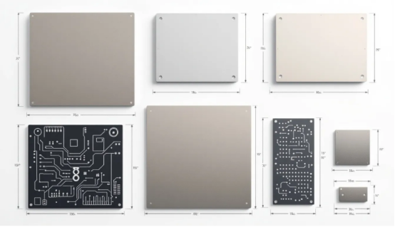
Standard PCB sizes are fundamental in the PCB industry, offering a benchmark for design and manufacturing. Common thicknesses like 1.57 mm, 2.36 mm, and 3.18 mm are prevalent in electronic applications, ensuring both compatibility and reliability. These thicknesses correspond to 100%, 150%, and 200% of the 1.57 mm standard, respectively, catering to different design requirements.
Standard panel sizes such as 18”x24” and 18”x12” are essential for maximizing production efficiency and yield. Knowing these dimensions allows PCB designers to optimize board size for both functionality and manufacturability.
Common Board Thicknesses
A typical PCB has a standard pcb thickness of 1.57 mm, commonly used in electronic applications. This thickness is vital in assembly, impacting design and component compatibility. However, some standardized interfaces utilize a thickness of 1 mm instead of the typical 1.57 mm, catering to specific design requirements.
These standard thicknesses ensure circuit boards can endure mechanical stress while maintaining electrical performance. The thickness choice affects the finished copper thickness, influencing overall design and functionality, including board thickness.
Standard Panel Sizes
Standard panel sizes include:
·18”x24”
·18”x12”
·9”x24”
·9”x12” panel size
These sizes are key for maximizing production efficiency and yield. Adjusting board size can significantly affect production yield, increasing the number of boards produced from each panel. This optimization not only reduces material waste but also enhances the overall cost-effectiveness of the manufacturing process, up to the maximum size allowed.
Adhering to these standard panel sizes allows PCB manufacturers to maintain consistent quality and efficiency in high-volume production.
Factors Affecting PCB Size
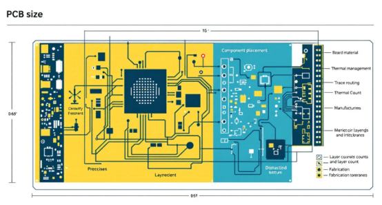
Various design choices, including component arrangement and type, as well as manufacturing limitations, influence PCB size. Reducing PCB dimensions can enhance portability but may limit space for components, affecting functionality. Maximizing PCB size efficiency requires a careful balance between component density and functionality.
PCB dimensions significantly influence its electrical conductivity and heat dissipation, impacting overall performance. Two critical factors are component density and routing/spacing.
Component Density
Higher component density often results in a more compact PCB layout, impacting size and design complexity. This density requires careful layout planning to minimize signal interference and thermal issues.
As component numbers increase, efficient space utilization becomes crucial. Designers must strategically place components to avoid overcrowding, which can cause overheating and signal degradation. By optimizing component density, designers can achieve a compact and functional PCB design.
Routing and Spacing
Routing paths and trace spacing are critical for ensuring effective electrical performance and manufacturability. Adequate spacing prevents electrical failures and facilitates manufacturability. Effective routing and proper spacing are vital to avoid manufacturing defects in densely populated PCBs.
Proper routing and trace spacing are essential to avoid electrical interference and ensure effective signal transmission. These practices maintain the integrity and reliability of the circuit board.
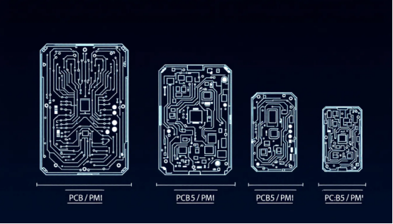
Custom PCB Sizes
Custom PCBs can be designed in various shapes to fit specific enclosures, enhancing integration with electronic components. Such designs accommodate unique dimensions and shapes, meeting specific application requirements. Handling custom designs and materials is a crucial factor in choosing a PCB manufacturer.
Custom PCB sizes offer flexibility but introduce complexities in design and manufacturing. Considerations for odd shapes and sizes, as well as associated costs, are important for each pad.
Odd Shapes and Sizes
Custom PCB designs are crucial for accommodating unique enclosure shapes, ensuring functional integration in devices. These designs must align with specific enclosures, necessitating unique dimensions and layouts for compatibility.
Higher component density usually requires a larger board to accommodate additional space for components and connections. More layers can fit complex circuits into a smaller footprint by stacking components vertically, optimizing the height ratio.
Strategic component placement reduces overall PCB size by minimizing trace lengths and optimizing space.
Cost Considerations
PCB size significantly influences manufacturing costs in the following ways:
·Larger boards typically incur higher material and production expenses.
·Larger PCBs often result in more material waste, especially when cut from standard panel sizes.
·Deviating from standard sizes complicates the manufacturing process, potentially increasing production timelines and costs.
Understanding these low cost considerations helps designers balance functionality with budget constraints.
Impact of PCB Size on Performance
PCB size intricately links to its electrical and thermal performance. Incorporating design rules and guidelines ensures size reduction doesn’t sacrifice performance. Thermal performance is influenced by size; larger PCBs distribute heat more effectively due to greater surface area, while smaller PCBs may struggle with heat dissipation, risking component overheating.
We will explore the impact of PCB size on electrical properties and thermal management.
Electrical Properties
PCB size affects resistance and inductance in the following ways:
·Larger boards can have lower resistance due to increased trace width.
·Larger PCBs generally show lower resistance because of increased copper surface area, which enhances conductivity.
·Copper thickness, which varies with board size, crucially determines the PCB’s electrical characteristics.
Larger PCBs with wider traces typically exhibit reduced electrical resistance, enhancing overall performance. Optimizing these properties ensures reliable circuit operation.
Thermal Management
PCB size impacts its heat dissipation ability; larger PCBs distribute heat more effectively due to greater surface area, while smaller ones may struggle, risking component overheating. Additional copper layers in a PCB enhance its thermal management capabilities, especially in larger designs.
Key points about PCB design and thermal management include:
·Vias in PCBs facilitate heat transfer, enhancing overall thermal performance.
·Blind and buried vias allow internal connections without using surface area.
·Higher component density allows for more features in a compact design but complicates heat management and routing traces.
Maintaining adequate spacing between traces and pads is crucial to prevent electrical interference and ensure effective heat dissipation.
Optimizing PCB Design for Size
Custom PCBs can be tailored to specific requirements, allowing designers to optimize performance for unique applications. Strategies for optimizing PCB design include layer stackup, component placement, and via usage in printed circuit boards, including single sided pcbs and pcb assembly.
Implementing these strategies enables designers to create efficient and functional PCB designs that meet specific application needs, for example, integrated circuits.
Layer Stackup
Using multiple layers in PCB design manages complex circuits while minimizing the board’s footprint. Copper layers are crucial for managing heat distribution, especially in larger designs. Trace thickness is vital for preventing overheating and maintaining sufficient current flow, particularly when considering the inner layers, outer layers, of the plated board, the copper clad laminate, and copper plating.
Careful layer stackup planning allows designers to optimize space and enhance circuit board performance, including the outer layer, internal layers, the inner layer, and solder mask.
Component Placement
Organizing components into functional blocks offers several benefits:
·Simplifies routing
·Minimizes interference in compact PCB designs
·Significantly reduces board size by minimizing space between elements
·Enhances circuit functionality through effective component placement
Efficient component placement optimizes board size, improves performance, and reduces manufacturing complexities. Focusing on component placement allows designers to achieve a streamlined and effective PCB layout.
Via Types and Usage
Different types of vias, like blind and buried vias, save space and enhance circuit performance. Thermal vias provide efficient heat transfer, improving thermal management in various board sizes and reducing the number of holes needed.
Utilizing the appropriate via types allows designers to optimize space and improve PCB functionality. This strategic use of vias manages complex routing and ensures effective heat dissipation.
Manufacturing Constraints and PCB Size
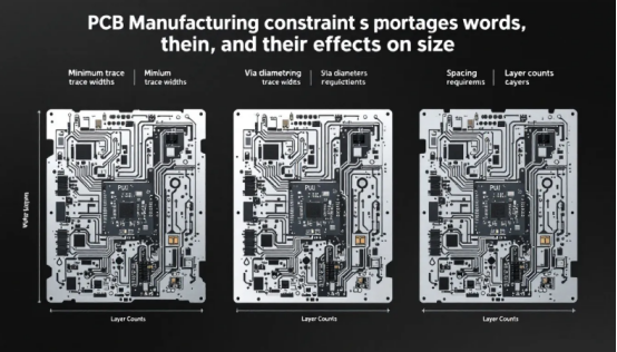
PCB size is often limited by the manufacturing equipment used. Precision in manufacturing processes is crucial to avoid defects from using sizes too small for the available technology. Advanced machinery and technology at a manufacturing facility can greatly enhance production efficiency.
A minimum clearance of ½ inch around PCB panels is necessary for handling, with 1 inch recommended for multilayer boards. We will explore the constraints imposed by:
·CNC routing
·V-cut
·Drill diameter
·Hole size on PCB manufacturing.
CNC Routing and V-Cut
CNC routing defines the edge of a PCB and ensures accurate panelization. This process achieves precise edges on PCBs, affecting overall aesthetics and functionality. Tab routing and V-cut techniques separate individual boards from a panel, ensuring clean and accurate cuts.
Understanding these manufacturing techniques allows designers to create PCBs that meet precise specifications and maintain high-quality standards.
Drill Diameter and Hole Size
Drill diameter and hole size are crucial aspects determining the feasibility of various PCB dimensions:
·Drill size directly affects design possibilities and overall PCB functionality.
·Minimum drill sizes typically begin at around 0.2 mm for standard PCB fabrication.
·Drill size impacts design flexibility.
Drill hole size can significantly affect PCB design and layout. Understanding these parameters is essential to determine informed design choices, ensuring manufacturability and performance.
Choosing the Right PCB Manufacturer
Selecting the right PCB manufacturer is crucial for ensuring circuit board quality and reliability. Manufacturers often use certifications like ISO 9001 to guarantee adherence to quality management standards. Component sourcing and verification ensure high-quality parts are used in PCB manufacturing.
Quality assurance in PCB manufacturing ensures products meet specified performance and reliability standards. We will discuss the capabilities and equipment of manufacturers, and the importance of quality control.
Capabilities and Equipment
Manufacturers like PCBMASTER support various materials including:
·FR-4
·Aluminum
·Copper Base These materials are essential for different PCB applications. If custom boards exceed the listed capabilities of a manufacturer like PCBMASTER, it is advisable to contact a sales representative for guidance.
PCBMASTER does not charge extra for standard colors (like Green, Red, Yellow, Blue) and other basic colors (like White and Black), making their customization options cost-effective. By choosing a manufacturer with the right capabilities and equipment, designers can ensure their PCBs meet the desired specifications and performance standards.
Quality Control
Quality control is crucial in PCB production to ensure the reliability and performance of the boards in various applications. Choosing a PCB manufacturer with appropriate capabilities and equipment is essential for maintaining high-quality standards during production.
High-volume production requires stringent quality checks to prevent defects and ensure consistency in the final product. By prioritizing quality control, manufacturers can deliver circuit boards that meet the rigorous demands of modern electronic devices.
Summary
Understanding PCB size is fundamental to optimizing design, performance, and cost. Standard PCB sizes provide a reliable foundation, while custom sizes offer flexibility for unique applications. Factors such as component density, routing, and manufacturing constraints play a crucial role in determining the optimal board size. By carefully considering these elements, designers can create efficient and high-performing circuit boards. Choosing the right manufacturer, with the necessary capabilities and stringent quality control, ensures the production of reliable and effective PCBs.
FAQs
Q.What are the common thicknesses for PCBs?
A.Common PCB thicknesses include 1.57 mm, 2.36 mm, and 3.18 mm, reflecting industry standardization. These measurements are crucial for ensuring compatibility in electronic applications.
Q.Why are standard panel sizes important in PCB manufacturing?
A.Standard panel sizes are vital in PCB manufacturing as they enhance production efficiency and yield, allowing for optimal use of materials and streamlined processing. Adhering to these sizes minimizes waste and supports consistent quality in the final products.
Q.How does component density affect PCB size?
A.Higher component density results in a more compact PCB layout, ultimately reducing the overall size and increasing design complexity.
Q.What role does CNC routing play in PCB manufacturing?
A.CNC routing is essential in PCB manufacturing as it precisely defines the edges and facilitates accurate panelization, impacting both the aesthetics and functionality of the final product.
Q.Why is quality control important in PCB manufacturing?
A.Quality control is essential in PCB manufacturing as it ensures the reliability and performance of the boards, adhering to stringent quality standards during production. This process ultimately protects against failures in various applications, reinforcing trust in the product's efficacy.
Author: Jack Wang

