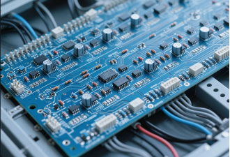
A Detailed Explanation of the PCB Assembly Production Process
I. Basic Definition of PCB Assembly
·PCB Assembly refers to the process of assembling electronic components (such as resistors, capacitors, chips, connectors, etc.) onto a PCB through soldering or mechanical fixation, ultimately forming a complete electronic module with full electrical functionalit board" to "functional module," encompassing a series of procedures from component preparation to final testing. It is a comprehensive application of processes such as SMT (Surface-Mount Technology), THT (Through-hole Technology), bonding, and Press-Fit.
II. Main Stages of PCB Assembly
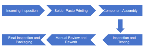
·The PCB Assembly process selects the process route based on product design (such as component type, PCB structure). The core stages include:
1.Incoming Quality Control (IQC)
·PCB Bare Board Inspection: Inspects the unassembled PCB for appearance and performance, such as checking if pads are oxidized, for scratches, and if conductivity is normal, ensuring the bare board quality meets assembly requirements.
·Component Selection: Screens components that meet specifications according to design documents (BOM list), including model, parameters, and package.
·Component Pre-processing: Performs pin forming, cleaning (removing oxide layer), taping/reeling (for automated placement) on some components to ensure solderability.
2.Solder Paste Printing (Core Step of SMT Process)
·For surface-mount components, solder paste (solder powder + flux) is precisely printed onto the PCB pads through a stencil, providing the medium for subsequent soldering. The quality of this stage directly affects solder joint reliability (e.g., solder paste volume, positional accuracy).
3.Component Assembly
·SMT Placement: Uses a pick-and-place machine to accurately place surface-mount components (e.g., 0402 resistors, QFP chips) onto pads printed with solder paste. Machine vision positioning (recognizing Mark points on the PCB) ensures placement accuracy. After placement, the PCB is heated in a reflow oven to melt the solder paste, wetting the pads and component leads/pins, forming solder joints upon cooling.
·THT Insertion: For components requiring through-hole soldering (e.g., connectors, high-power resistors), pins are inserted into the PCB's through-holes manually or by an automatic insertion machine. This is suitable for scenarios requiring higher mechanical strength. After insertion, soldering is performed using wave soldering equipment, selective wave soldering equipment, or manual soldering to fill the through-holes with solder and form solder joints.
·Bonding: Wire bonding process used in chip production to connect the internal circuit of the chip to the package pins or PCB gold-plated copper foil before encapsulation. An ultrasonic generator produces 40-140KHz ultrasound, transmitted through a transducer and horn to the bonding wedge. When the wedge contacts the lead wire and the bonding pad, under pressure and vibration, friction destroys the oxide layer on the metal surface, causing plastic deformation. Pure metal surfaces come into close contact, forming an atomic-level bond to achieve a firm mechanical connection. After connecting the circuit to the pins, the chip is typically encapsulated with black epoxy.
·Press Fit: A solderless THT technology that uses mechanical force to precisely press the pins of a Press Fit connector into the PCB's Press Fit holes, achieving electrical connection through mechanical force.
4. Inspection and Testing
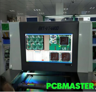
·AOI (Automated Optical Inspection): Uses cameras to inspect soldering quality (e.g., shorts, insufficient solder, missing/misplaced components).
·X-Ray Inspection: Inspects the soldering quality of hidden solder joints (e.g., under BGA chips).
·ICT (In-Circuit Test): Uses a bed-of-nails tester to check for opens, shorts, component values, etc., in the circuit.
·FCT (Functional Test): Simulates actual working conditions to test whether the fully assembled PCBA's complete functions are normal.
5. Manual Review and Rework:
·Manually repair defects identified during inspection (e.g., insufficient solder, bridging, missing components), such as resoldering or replacing components.
6. Final Inspection and Packaging:
·After completing all processes, perform final inspection and package properly.
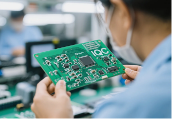
Having worked deeply in the electronic manufacturing field for many years, PCBMASTER understands well: the starting point of high-quality products is not the production line, but the IQC workstation. As the "gatekeeper" of the entire PCB Assembly process, IQC's core mission is to intercept non-conforming materials, preventing production stoppages, batch rework, and customer complaints caused by "source contamination." Below is PCBMASTER's full-process IQC standard, refined from experience collaborating with thousands of clients. From receiving and verification to risk control, every step carries the commitment to "zero defects."
I. IQC Core Work Content: Full-Chain Control from Receipt to Disposition
1. Material Receiving and Verification: Guarding the "First Gate"
·Three-Document Matching: Strictly verify the "six consistencies" between the delivery note, purchase order, and supplier label – material code, specification/model, batch number, quantity, environmental marking (RoHS/HF), and supplier information – ensuring source information is accurate (PCBMASTER's exclusive "Three-Document Smart Matching System" achieves 99.9% automatic verification).
·Packaging Inspection: Focuses on checking anti-static packaging (resistance value 10⁶-10¹¹Ω), status of Moisture Sensitive Devices' (MSD) Humidity Indicator Cards (HIC) (<10% is qualified), fragile item markings, and storage condition labels. Materials with damaged/damp outer packaging directly initiate the isolation procedure.
·Inspection Level Determination: According to the "PCBMASTER Material Risk Grading Standard," materials are divided into three categories: A (core chips / BGA), B (resistors/capacitors), C (auxiliary materials). Category A materials undergo 100% full inspection, Category B are sampled according to MIL-STD-1916, Category C are exempt (requires supplier to have zero non-conformances for 12 consecutive months).
2. Sampling: Making "Samples" Represent the "Entire Batch"
·Standard Execution: Adopts a dual-track system of "International Standard + Internal Algorithm" – basic sampling follows ANSI/ASQ Z1.4, while adding the PCBMASTER Risk Coefficient (e.g., first order from a new supplier tightened by 2 levels, materials with historical defect rate >5% tightened by 1 level).
·Scientific Sampling: Samples are taken from different cartons and different stacking positions within cartons (at least 3 locations per carton), ensuring coverage of "edge" and "center" materials. Sampling records are uploaded to the MES system in real-time, enabling full traceability from "sample" to "batch."
3.Inspection and Testing: "Microscopic-Level" Scrutiny at the Core Stage
PCBMASTER develops differentiated inspection plans based on material type. Key items are as follows:
Material Type | Key Inspection Items (Based on "PCBMASTER Inspection Specification V3.0") | Inspection Tools |
Electronic Components | Pins: Flatness (≤0.05mm deviation), Oxidation Level (tested via SEM scanning electron microscope, oxide layer ≤0.03μm); Body: Marking Clarity (laser marking must withstand alcohol wipe 3 times without fading), Package Dimensions (deviation from approval doc ≤0.1mm) | 2D Optical Comparator, Microscope, Pin Coplanarity Tester |
PCB/PCBA | Board Surface: Scratches (depth ≤1/3 copper thickness), Exposed Copper (not allowed), Warpage (≤0.75%); Pads: Contamination/Oxidation (verified by solderability test); Hole Position Accuracy (±0.02mm) | AOI Optical Inspector, Laser Thickness Gauge, Pull Tester |
Process Materials | Solder Paste: Metal Content (32-35%), Viscosity (150-200Pa・s, 25℃); Red Glue: Shear Strength after Curing (≥15N) | Solder Paste Viscometer, Thermogravimetric Analyzer (TGA) |
Stencil / Carrier Tape | Stencil Tension (≥30N/cm), Aperture Size (deviation from Gerber ≤0.01mm); Carrier Tape Cover Tape Adhesion (3-8N/25mm) | Stencil Tension Meter, Image Measuring Instrument |
4. Disposition and Handling: Clear Classification, Rapid Response
·Disposition Standard: According to "PCBMASTER Accept/Reject Criteria," Category A materials have zero tolerance (e.g., BGA solder ball voiding >5% directly rejected), Category B materials allow extremely minor cosmetic defects (must not affect function).
·Handling Process:
ü ·Conforming: Affix green "PASS" label, simultaneously unlock MES system warehouse permission.
ü ·Non-conforming: Affix red "REJECT" label + store in locked isolation area, generate "8D Corrective Action Report" within 2 hours and synchronize with supplier and internal SQE team.
ü ·Use As Is (UAI): Requires review by "Quality + Engineering + Production" departments, specifying usage restrictions (e.g., limited to a specific order) and marked with a blue "UAI" label for full traceability.
II. PCBMASTER IQC Key Precautions: Details Determine Success or Failure
1. Special Control for "High-Risk Materials"
·New Materials / New Suppliers: First order undergoes "Full Inspection + Reliability Testing" (e.g., temperature cycling -40℃~125℃, 100 cycles without abnormality).
·Moisture Sensitive Devices (MSD): Inspection must be completed within 4 hours of unpacking. If unused beyond this time, initiate baking immediately (PCBMASTER's unique "MSD Time Limit Warning System" alarms 30 minutes beforehand).
·Core Chips: Extract 3pcs per batch for X-Ray inspection to verify internal solder joint / gold wire connection status.
2. ESD and Environmental Control: The "Safety Net" in Details
·EPA Area Management: Inspection table mats, wrist straps, and flooring must be tested daily (resistance value 10⁶-10⁹Ω), equipped with anti-static handling boxes (surface resistance 10⁷Ω).
·Temperature & Humidity Control: MSD inspection area constant temperature 23±2℃, humidity 40-60%, equipped with automatic dehumidifier (response time <5 minutes).
3. Record Traceability: Making Every Batch "Traceable"
·Inspection records must include: Inspector, Equipment ID (including calibration status), Inspection Time, Key Parameters (e.g., solder paste viscosity value), Defect photos (with timestamp). All data saved for at least 3 years (10 years for automotive electronics projects), retrievable via batch number with one click.
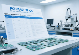
III. PCBMASTER IQC Core Specifications: Systematic Guarantee of "Zero Defects"
1. Document System: Standardization as the "Iron Rule"
·Core Documents: "PCBMASTER IQC Work Instruction V3.0", "Material Risk Grading Standard", "MSD Component Management Specification", updated annually (incorporating customer feedback and industry standard updates).
·Sample Management: Establish a "Golden Sample Library" (including components / PCB / auxiliary materials), each sample marked with "Validity Period" and "Decision Boundary" (e.g., limit samples for "acceptable/unacceptable" cosmetic defects on resistors).
2. Equipment Management: Precision is the "Hard Guarantee"
·All inspection equipment (e.g., 2D Optical Comparator, LCR meter) calibrated by CNAS-accredited institutions. Calibration cycle: Precision instruments every 6 months, regular tools every 12 months. Calibration certificates uploaded to QMS system in real-time.
3. Continuous Improvement: Data-Driven "Upgrade Iteration"
·Publish monthly "IQC Quality Monthly Report," analyzing TOP 3 defects (e.g., pin oxidation, PCB warpage), TOP 3 problematic suppliers, driving supplier corrective actions (e.g., PCBMASTER initiates on-site audits for suppliers with defect rates >3% for 3 consecutive months).
·Encourage inspectors to submit "Improvement Proposals." 23 proposals adopted in the past 3 years (e.g., "MSD Baking Time Auto Calculator," "ESD Packaging Rapid Test Method"), improving IQC efficiency by 40%.
IV. IQC is the Starting Point of the "Quality Ecosystem"
·At PCBMASTER, IQC is not simply about "finding faults," but a link to building a "Quality Community" with suppliers. From resistors and capacitors to chips and PCBs, every batch's inspection report carries the promise of "putting customers at ease." Choosing PCBMASTER is not just choosing a manufacturing service provider, but choosing a full-process quality assurance system covering "incoming material - production - delivery" – because we deeply understand: guarding IQC is guarding customer trust.
PCB Loading and Solder Paste Printing Work Content, Precautions, and Specifications

I. PCB Loading Work Content
1. Pre-operation Preparation
·Material Verification: Retrieve corresponding PCB boards based on the production work order, verify model, batch number, quantity consistency with the order, inspect PCB appearance (referencing IQC inspection standards), confirm absence of oxidation, deformation, circuit damage, etc. Fill out the "PCB Material Receipt Verification Checklist."
·Equipment Check: Confirm the loading machine (or manual loading station) conveyor rail width matches the PCB size, positioning pins and sensors are working normally, ESD protection devices (rail grounding, workstation ionizer) are effective. Record in the "Equipment Daily Checklist."
·Tool Preparation: Prepare anti-static tweezers, positioning fixtures, lint-free wipes (dipped in IPA), ensuring tools are clean and free of foreign objects.
2.Loading Operation Process
·Unpacking and Cleaning: Remove PCB packaging, gently wipe board edges with a lint-free wipe (avoid touching pads) to remove surface dust; if vacuum packed, loading must be completed within 30 minutes of unpacking to prevent secondary contamination.
·Positioning and Placement: Place the PCB board smoothly along the conveyor rail, ensuring board edges align with the positioning reference (deviation ≤0.1mm). For manual loading, gently push until positioning pins are engaged, avoiding impact on rail edges.
·Fixing and Detection: Start the conveyor device. Once the PCB reaches the printing station, confirm vacuum suction (suction force 0.4-0.6MPa) or mechanical clamping is secure. Use the vision positioning system to detect board position offset (allowable deviation ≤0.05mm). If offset exceeds limit, stop machine for adjustment.
II. Solder Paste Printing Work Content
1. Solder Paste Management
·Storage and Retrieval: Solder paste must be stored in a 2-8℃ refrigerator. Retrieve using "First-In-First-Out" principle. Record retrieval date, batch number, remaining quantity. Fill out the "Solder Paste Storage & Retrieval Record." After retrieval, temper at room temperature (23±2℃) for at least 4 hours. Heating for tempering is prohibited. Mark tempering completion time after tempering.
·Stirring: Stir tempered solder paste using an automatic mixer (speed 1000-1500r/min, time 2-3 minutes) or manually (in the same direction, time 5-8 minutes), ensuring paste is uniform and bubble-free. Measure viscosity after stirring (300-500Pa・s, 25℃). Record in the "Solder Paste Stirring Inspection Record."
2. Printing Parameter Setup and Debugging
·Stencil Preparation: Select the corresponding stencil based on the PCB pad design. Check stencil aperture size (match with pads ≥90%), aperture wall smoothness. Clean both sides of the stencil with IPA-dipped lint-free wipes. Confirm no residual solder paste or foreign objects. Fill out the "Stencil Cleaning Checklist."
·Parameter Setting: Set printing parameters according to the process document: Squeegee pressure (5-15N), Print speed (20-50mm/s), Squeegee angle (45°-60°), Stencil-PCB separation gap (0.1-0.3mm), Separation speed (1-3mm/s). Parameters must be confirmed by the process engineer after setting. Record in the "Solder Paste Printing Parameter Setting Sheet."
3. Printing Operation and Inspection
·Test Print and Calibration: Before printing the first PCB, perform test prints (3 consecutive boards). Inspect solder paste coverage on pads (≥95%) under 20x magnification, checking for defects like insufficient solder, excess solder, bridging, or misalignment. Use a solder paste thickness gauge to measure thickness (within ±10% of design value). After the first piece passes, affix a "First Piece Qualified" label. Fill out the "First Article Inspection Report."
·Batch Printing: Start the automatic printer. Clean the stencil once every 50 PCBs printed (dry wipe + wet wipe + dry wipe), record cleaning time. During printing, sample 1 PCB every 30 minutes. Use SPI (Solder Paste Inspection machine) to detect solder paste shape, thickness, and offset. Data uploaded to MES system in real-time.
4. Solder Paste Printing Defects and Solutions
Insufficient Solder
·Phenomenon: Solder paste coverage area on pad less than 90%, localized voids appear.
· Causes: Stencil aperture clogged or deformed; Squeegee pressure too low; Solder paste viscosity too high; Stencil-PCB gap too large.
·Solutions: Clean stencil apertures or replace stencil; Appropriately increase squeegee pressure (each adjustment increment ≤2N); Re-stir solder paste to lower viscosity; Reduce Stencil-PCB gap (adjustment amount ≤0.05mm).
Excess Solder
·Phenomenon: Solder paste exceeds pad edge, thickness exceeds design value by more than 10%.
· Causes: Squeegee pressure too high; Print speed too slow; Stencil aperture size too large; Solder paste viscosity too low.
·Solutions: Reduce squeegee pressure; Increase print speed (each adjustment increment ≤5mm/s); Replace with matching stencil; Add appropriate amount of solder paste thinner (as per instructions).
Bridging
· Phenomenon: Solder paste connects adjacent pads into a single mass.
· Causes: Stencil aperture spacing too small; Squeegee angle too small; Separation speed too slow; PCB pad spacing design unreasonable.
·Solutions: Replace stencil with compliant aperture spacing; Increase squeegee angle (adjust to 50°-60°); Increase separation speed; Feedback to process engineering department to evaluate pad design optimization.
Misalignment
·Phenomenon: Solder paste center deviates from pad center by more than 0.1mm.
·Causes: PCB positioning inaccurate; Stencil-PCB alignment deviation; Conveyor rail loose.
·Solutions: Recalibrate PCB positioning fixture; Adjust stencil alignment parameters; Tighten conveyor rail screws and calibrate parallelism.
Solder Balls
·Phenomenon: Tiny solder particles (diameter ≥0.2mm) appear on pad edges or PCB surface.
·Causes: Residual solder paste under stencil; PCB pad oxidation; Excessive flux content in solder paste; Excessive time between printing and placement.
·Solutions: Strengthen stencil cleaning (increase wet wipe frequency); Reprocess PCB pads (sanding or cleaning); Change solder paste batch; Shorten interval between printing and placement (control within 2 hours).
Pinholes / Voids
·Phenomenon: Holes (diameter ≥0.1mm) appear on solder paste surface.
·Causes: Inadequate solder paste stirring, entrapped air; Printing environment humidity too low (<40%); Stencil aperture inner wall not smooth.
·Solutions: Extend stirring time (add 1 minute for automatic stirring); Increase ambient humidity (turn on humidifier); Replace stencil with smooth aperture walls.
III. Precautions
1.ESD Control: Operators must wear tested and qualified anti-static wrist straps and anti-static clothing. PCBs must be placed on anti-static trays. Direct contact with pads and circuits is prohibited.
2.Solder Paste Protection: Avoid exposing solder paste to air for more than 1 hour during use (prevents moisture absorption). Unused solder paste must be marked with usage count (maximum 2 reuses). Mixing with new solder paste is prohibited. Discarded solder paste must be collected according to hazardous waste procedures.
3.Equipment Safety: Press the emergency stop button when adjusting the printer. Touching moving parts like the squeegee or stencil during operation is prohibited. Regularly clean the squeegee (every 8 hours) to prevent solder paste curing affecting print quality.
4.Environmental Control: Maintain a clean printing area (Class 10000), temperature (23±2℃), relative humidity (45%-65%). Monitor and record daily. Excessive humidity can cause solder paste to absorb moisture; too low humidity can generate static electricity.
IV. Operation Specifications
·Parameter Management: Printing parameters must be approved and archived by the Process Engineering department. Any parameter change requires filling out a "Parameter Change Request Form" and execution only after engineer approval. Old parameters archived for 3 years.
·Recording Requirements: Fill out the "Solder Paste Printing Production Record Sheet" per shift, including PCB model, solder paste batch, printed quantity, yield, abnormalities (e.g., bridging, insufficient solder) and actions taken. SPI inspection data must be named/stored by "Hour + Equipment ID," traceable to specific PCB serial numbers.
·Abnormality Handling: If solder paste printing defects are found (e.g., bridging occurs on 3 consecutive boards), immediately stop the machine to check stencil apertures (for blockage/deformation), squeegee pressure (for uniformity), PCB positioning (for offset). After handling, re-run a test first piece. Only resume production after it passes. Fill out an "Abnormality Handling Form."
·Shift Handover Specification: During shift handover, confirm solder paste remaining quantity, equipment status, and unresolved abnormalities face-to-face. Sign confirmation on the "Shift Handover Record Sheet" to ensure no information gaps.
SPI Solder Paste Inspection: Definition, Principle, Role, and Process
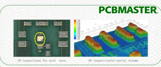
·In the SMT production process, solder paste printing is the key step determining soldering quality. SPI (Solder Paste Inspection) is the core process for precisely inspecting solder paste quality after printing, acting as the "gatekeeper" ensuring subsequent soldering yield. The following explains in detail from four aspects: definition, principle, role, and process.
I. Definition of SPI Solder Paste Inspection
·SPI Solder Paste Inspection refers to the automated inspection technology that uses optical inspection equipment to measure three-dimensional or two-dimensional parameters of solder paste printed on a PCB, comparing them with preset standards to determine if solder paste printing defects exist (such as insufficient solder, excess solder, misalignment, bridging, etc.).
·It is the intermediate quality control point in the SMT production flow of "Solder Paste Printing → SPI Inspection → Component Placement," enabling early detection of printing issues before soldering, preventing defects from flowing into subsequent processes.
II. Main Principle of SPI Solder Paste Inspection
·The core principle of SPI is optical imaging and 3D reconstruction technology. Mainstream is now 3D SPI (more accurate than traditional 2D SPI). The specific process is as follows:
1.Optical Scanning:
·The equipment projects structured light (e.g., laser lines, fringe patterns, or multi-frequency gratings) onto the printed surface of the PCB through a projection module. Simultaneously, high-resolution cameras (multi-angle) capture the reflected/scattered light signals from the solder paste surface.
2.3D Reconstruction:
·Uses "triangulation" to calculate the 3D morphology of the solder paste: The projected light forms distorted patterns on the solder paste surface. After capturing the distorted image, algorithms analyze the pattern shift to calculate solder paste height, volume, surface area, and other 3D parameters (2D SPI can only detect area through grayscale values, unable to determine height and volume, gradually being replaced by 3D).
3.Data Comparison:
·Compares the measured 3D parameters (e.g., solder paste volume, height, area, offset, bridging spacing) with preset standard templates (set based on PCB pad design parameters). Anything outside the tolerance range is judged as a defect.
III. Role of SPI Solder Paste Inspection
SPI is the "core defense line" of SMT quality control. Its main roles include:
1.Timely Interception of Printing Defects:
·Accurately identifies defects like insufficient solder (low volume), excess solder (excess volume), misalignment (position deviation), bridging (solder paste connecting adjacent pads), pinholes (holes in solder paste surface), preventing these issues from causing subsequent soldering defects (e.g., cold solder joints, false soldering, shorts).
2.Improve Production Yield and Efficiency:
·Compared to manual sampling (low efficiency, high missed detection rate), SPI can perform 100% full inspection, with defect detection rates above 99%, reducing batch rework caused by printing issues, lowering material waste and labor costs.
3.Optimize Printing Process Parameters:
·By statistically analyzing defect types (e.g., high proportion of excess solder in a batch) and distribution patterns (e.g., frequent misalignment in a specific area), it provides feedback to guide adjustments in solder paste printing parameters (e.g., squeegee pressure, speed, stencil aperture size), enabling continuous improvement of process stability.
4.Data Traceability and Process Control:
·Records inspection data for each PCB (defect type, location, parameter deviation value), supporting quality traceability (e.g., tracing printing quality of a specific PCB batch), while also providing data support for SPC (Statistical Process Control) in the production process.
IV. Process of SPI Solder Paste Inspection
The SPI inspection process needs to be integrated with the SMT line, embedded between printing and placement. Specific steps are as follows:
1.PCB Positioning and Pre-processing
·The PCB enters the SPI inspection station via conveyor. The equipment achieves precise positioning by recognizing Mark points (fiducials) on the PCB, ensuring detection positions match pad coordinates (positioning accuracy ≤±0.01mm).
·Some equipment performs surface cleaning (e.g., air blow) first to avoid PCB surface contaminants (e.g., solder paste debris) interfering with imaging.
3D Scanning and Imaging
·The equipment initiates optical scanning: The projection module projects structured light while cameras simultaneously capture 3D images of the solder paste surface, generating a 3D model of the solder paste for each pad (including X/Y position, Z-axis height data).
·Scanning speed is adjusted based on PCB size. Typically, inspection time for a single PCB (e.g., 300×200mm) is ≤2 seconds, matching the production line cycle time.
Data Processing and Defect Judgment
·Algorithms analyze the scan data: Calculate key parameters for each pad, such as solder paste volume (core indicator, typically required within ±15% of standard value), height (avoid insufficient height causing cold joints), area (avoid insufficient coverage), offset (X/Y direction deviation ≤0.1mm).
·Compare with preset standard templates. Parameters exceeding tolerance are judged as defects and classified by severity (e.g., critical defect: bridging; minor defect: slight offset).
Result Feedback and Handling
·If the inspection passes, the PCB proceeds to the next process (component placement) via conveyor. If defects exist, the equipment alerts the operator via audible/visual alarms, displays defect location and parameter deviation (e.g., "Pad R12 Volume -20%") on the screen, and may mark the defective PCB (e.g., via dot marking).
·The operator can view defect images (3D visualization) via the equipment interface to determine if rework is needed (e.g., manual solder touch-up, wiping excess paste).
Data Storage and Statistical Analysis
·Inspection data is automatically uploaded to the MES system, generating daily/weekly reports (e.g., defect rate, TOP3 defect types), enabling production managers to monitor printing process stability and providing a basis for process optimization.
V. SPI Solder Paste Inspection is the key "preventative" link in SMT production.
·Through optical 3D inspection technology, it achieves precise identification, timely interception, and process optimization of printing defects. It is a core technological means to ensure soldering quality and improve production efficiency in electronic product manufacturing. In high-density, high-precision SMT production (e.g., mobile phones, automotive electronics), SPI has become an indispensable quality control device.
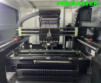
·SMT stands for "Surface Mount Technology." Simply put, it involves directly "mounting" electronic components onto the surface of a PCB, unlike traditional processes where component leads are inserted into through-holes in the PCB. This "hole-less" design allows components to be densely packed on the PCB – a smartphone motherboard less than 100 cm² can accommodate thousands of resistors, capacitors, and chips. This was unimaginable in the THT era. Therefore, in the SMT placement flow, the placement equipment (Pick and Place Machine) is the core for achieving "precision landing" of components. Its performance directly determines placement accuracy (±0.025mm level) and production efficiency (up to 100,000 points/hour). Below is a systematic explanation from the types of mainstream equipment used by PCBMASTER, core configurations, working logic, to operation specifications.
I. Mainstream Placement Equipment Types and Application Scenarios
Based on speed and accuracy, mainstream equipment is divided into three categories, adapting to different production needs:
Equipment Type | Core Characteristics | Typical Configuration Parameters | Application Scenarios |
High-Speed Placer | Focuses on mass production efficiency, placement speed >30,000 CPH (Components Per Hour) | 8-24 placement heads, feeder capacity >100 stations | Mass production of consumer electronics (e.g., mobile phone board resistors, capacitors) |
High-Precision Placer | Focuses on micro/miniature & precision components, accuracy ±0.01mm | 4-6 high-precision placement heads, AI vision system | Chip-level placement (BGA, QFP, 01005 components) |
Universal Placer | Balances speed and flexibility, capable of placing irregular components | 2-4 placement heads, supports tray/tube feeders | Small batch, high mix production (e.g., industrial sensors, medical devices) |
II. Core Configurations and Functions of Placement Equipment
The "Accuracy and Efficiency" of placement equipment are determined by the following core components:
Placement Head
·Structure: Six-axis articulated robotic arm (X/Y/Z axis movement, θ axis rotation, U/V axis fine adjustment), equipped with vacuum nozzles (diameter 0.3-5mm, adapting to different component sizes).
·Function: Picks up components via vacuum suction, releases vacuum and applies 0.1-5N pressure during placement (adjusted based on component weight to avoid damaging PCB or components).
·PCBMASTER Configuration: Uses YAMAHA equipment, response speed 0.02 seconds/action, supports automatic nozzle change (change time <0.5 seconds).
Vision Positioning System
·Composition: Top camera (identifies PCB Mark points) + bottom camera (identifies component leads/shape), resolution 5-20 Megapixels, coupled with AI algorithms (recognition speed >1000 components/second).
·Function: Real-time calibration of component offset (X/Y direction ±0.005mm, angle ±0.01°), automatic rejection of reversed, flipped, or bent-lead components.
Feeder System
·Types: Tape feeder (paper/plastic - resistors, capacitors), Tray feeder (IC chips), Tube feeder (connectors), supports 8mm-56mm tape widths.
·Features: Feeding accuracy ±0.02mm, includes automatic tape detection (stops and alarms for empty tape or tape runout).
Control System
Industrial PC + touch screen, supports offline programming (import Gerber/BOM files to automatically generate placement program), displays real-time placement yield, equipment status (OEE metrics).
III. Placement Equipment Workflow (Standardized Operation Steps)
1.Pre-Production Preparation
·Program Import: Generate placement program via offline programming software, setting component coordinates, nozzle type, placement pressure, etc. (e.g., 0.3mm nozzle for 01005 components, pressure 0.1N).
·Material Loading: Load reels/trays onto feeders. Scan barcodes to verify component model (prevent wrong parts). Ensure tape tension is uniform (avoid component shifting).
·Equipment Calibration: Calibrate placement head (X/Y axis deviation ≤0.01mm) and camera focus (ensure clear component recognition) using standard fixtures.
2.Online Placement
·Step 1: PCB enters equipment via conveyor. Top camera recognizes Mark points, calibrating PCB position (compensating for board warp, positioning error).
·Step 2: Placement head moves to feeder. Vacuum nozzle picks up component (suction pressure adjusted based on component weight, e.g., -50kPa for IC chips, -30kPa for resistors).
·Step 3: Bottom camera captures component image. AI algorithms compare with standard library, calculating offset (e.g., automatically compensates θ axis angle if component rotated 1.5°).
·Step 4: Placement head moves to target pad, places component with preset pressure (ensuring component bottom fully contacts solder paste, no floating).
·Step 5: Real-time statistics of placed quantity, yield. Auto-alarm and pause for specific head if tape empty/nozzle clogged (without affecting overall production).
3.Post-Production Check
·Sample first PCB, use AOI to detect placement offset (allowable deviation: Chip components ≤0.1mm, QFP leads ≤0.05mm), polarity errors, etc.
·Export production data (hourly placement quantity, defect type statistics) for equipment parameter optimization.
IV. Operation Precautions and Specifications
1.Equipment Maintenance Specifications
·Daily: Clean nozzles (remove solder paste residue with ultrasonic cleaner), check vacuum level (≥-80kPa, otherwise components may drop).
·Weekly: Calibrate placement head (detect X/Y axis positioning error with laser interferometer), lubricate drive rails (avoid mechanical wear affecting accuracy).
·Monthly: Replace feeder belts (prevent tape slippage), calibrate vision system (test recognition rate ≥99.95% with standard components).
2.Process Parameter Setting Taboos
·Prohibit using the same nozzle for different size components (e.g., 0.3mm nozzle placing 0402 components easily causes mis-pick).
·Placement pressure must not be too high (e.g., >2N for BGA chips may crush solder balls) nor too low (component floating easily causes soldering defects).
·Environment temperature/humidity control required (temp 20-26℃, humidity 40%-60%), avoid ESD (operators must wear grounded wrist straps, equipment grounding resistance ≤1Ω).
Emergency Handling
·Component Jam: Immediately press emergency stop button. Manually remove jammed component. Check if nozzle is worn (replace if cracked).
·Vision Recognition Failure: Check camera lens for dust (clean with IPA-dipped lint-free wipe), verify component library is updated (new components need 3D model input).
V. PCBMASTER Equipment Operation Standard (Example: High-Precision Placer)
To ensure ±0.025mm placement accuracy, PCBMASTER implements a "Three-Check, Three-Calibrate" system:
·Three-Check: First-piece self-check (operator), Patrol inspection (QC every 2 hours), Last-piece full check (process engineer).
·Three-Calibrate: Calibrate nozzle height at shift change, calibrate vision system per batch, calibrate placement pressure sensor weekly.
Through standardized operation, PCBMASTER achieves placement yield ≥99.8%, 01005 component placement offset ≤0.05mm, meeting high-reliability requirements for automotive electronics, medical devices, etc.
SMT Pre-Reflow AOI: A Key Link in SMT Quality Control
SMT (Surface Mount Technology) Pre-Reflow AOI (Automated Optical Inspection) is a critical quality control link in the SMT production process, primarily used for automatic optical inspection of PCBs (Printed Circuit Boards) after solder paste printing or after component placement. The following details its role, importance, and engineering process:
I. Role and Importance of SMT Pre-Reflow AOI
1. Core Roles
Solder Paste Printing Quality Inspection (Post-Printing AOI)
·Detects solder paste printing defects, such as insufficient print, excess print, missing print, misalignment, bridging (adjacent pads connected), shape abnormality, uneven thickness.
·Identifies PCB pad abnormalities, such as contamination, oxidation, damage, preventing soldering defects caused by pad issues.
Component Placement Quality Inspection (Post-Placement AOI)
Detects component placement defects, such as missing components, wrong components (incorrect model/specification), misalignment (placement offset from pad), skew, flipped components, floating (component not seated on paste), bent leads.
2. Importance
·Intercept Defects Early, Reduce Production Costs:
Pre-Reflow AOI is located before reflow soldering (oven soldering), enabling detection of printing or placement defects before soldering. If defects flow into reflow, they may cause irreversible issues like cold solder joints or bridging. Subsequent rework requires component removal (potentially damaging the PCB), costing far more than pre-reflow repair.
·Improve Production Efficiency, Reduce Batch Defects:
Automated inspection quickly identifies and locates defects, avoiding the missed detection and false calls of manual inspection. It also provides timely feedback to upstream processes (e.g., printer, placer) for rapid parameter adjustment (e.g., print pressure, placement accuracy), preventing batch defects.
·Ensure Product Reliability, Reduce After-Sales Risk:
Solder paste printing and placement defects are the main causes of soldering issues (accounting for over 60% of SMT defects). Pre-Reflow AOI strictly controls source quality, reducing equipment failures caused by cold joints, shorts, etc., enhancing end-product reliability, and lowering after-sales repair costs.
·Data Traceability and Process Optimization:
AOI equipment records inspection data (e.g., defect type, quantity, location, frequency). Data analysis can pinpoint weaknesses in upstream processes (e.g., a printer repeatedly causing misalignment), providing data support for process optimization and continuous improvement of production stability
II. Engineering Process of SMT Pre-Reflow AOI
The Pre-Reflow AOI process needs to connect with the SMT line sequence. The core process varies slightly based on the inspection point (post-printing or post-placement):
1. Preparation
·Program Creation: Create an inspection template in the AOI system based on the PCB's CAD files (e.g., Gerber, BOM list), defining inspection areas (pads, component positions) and defect judgment criteria (e.g., allowable offset range, bridging threshold).
·Parameter Calibration: Adjust camera lighting (bright field/dark field, color light), resolution, inspection speed, etc., based on PCB material, solder paste color, component type (e.g., 01005 miniature, QFP/QFN precision devices) to ensure image clarity and defect recognition accuracy.
2.Online Inspection Process
·Board Transfer: PCB enters the AOI equipment via conveyor. The equipment automatically locates the board (using PCB edges, tooling holes, or Mark points for calibration, ensuring inspection positions match the template).
·Optical Imaging: The equipment scans the PCB surface using high-resolution cameras (typically with multiple light sources, e.g., ring light, bar light), acquiring high-definition images (2D or 3D; 3D AOI can detect solder paste thickness, component floating).
·Image Comparison and Analysis: The system compares the real-time image with the preset template at the pixel level. Algorithms (e.g., grayscale analysis, geometric shape matching) identify abnormal areas and determine if they are defects (e.g., solder paste offset exceeding threshold is judged as "Offset Defect").
·Defect Classification and Marking: Detected defects are classified by type (e.g., bridging, missing component) and severity (e.g., critical defect, minor defect). Defect locations are displayed on the equipment screen (usually overlaid on the PCB image), and audible/visual alarms alert the operator.
3.Subsequent Handling
·Defect Confirmation and Sorting: The operator manually reviews defects displayed by the AOI (to rule out false calls). Confirmed defective boards are marked (e.g., with a reject label) and sorted to the rework area.
·Data Recording and Feedback: Equipment automatically uploads inspection data (board ID, defect info, inspection time) to the MES system (Manufacturing Execution System). It also feeds back parameter anomalies to upstream equipment (e.g., prompts printer to adjust squeegee pressure or stencil alignment if frequent misalignment occurs).
·Equipment Maintenance and Calibration: Regularly clean camera lenses and light sources, check conveyor accuracy. Update inspection programs based on PCB differences across production batches to ensure long-term stable operation.
III. Pre-Reflow AOI is the "first line of defense" in SMT quality control.
By accurately detecting printing and placement defects, it reduces production costs, improves efficiency, and provides data support for process optimization. It is a core link in ensuring SMT product quality. Its engineering process requires a combination of automated equipment and manual review to achieve "detection - feedback - improvement" closed-loop management.
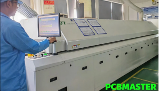
SMT Reflow Soldering: Meaning, Role, Oven Type Differences, and Related Introduction
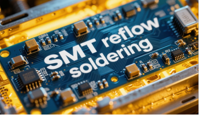
I. Meaning of SMT Reflow Soldering
·SMT Reflow Soldering is the core process in Surface Mount Technology (SMT) that achieves the electrical connection and mechanical fixation of components to PCB pads. Its principle involves heating the PCB with printed solder paste (composed of solder powder and flux) in a stepwise manner, causing the solder paste to undergo "melting - wetting - solidification." This ultimately forms reliable solder joints, permanently fixing surface-mount components (e.g., resistors, capacitors, chips) to the PCB.
·Reflow soldering is the key step in the SMT production line flow: "Solder Paste Printing → Component Placement → Pre-Reflow AOI Inspection → Reflow Soldering → Post-Reflow AOI Inspection." Located after Pre-Reflow AOI, it is the "forming step" that transforms the results of prior processes (qualified solder paste printing and component placement) into stable solder joints.
II. Main Roles of SMT Reflow Soldering
1.Achieve Reliable Electrical and Mechanical Connection:
·During reflow, the melted solder paste wets the PCB pads and component lead/pin surfaces, forming an intermetallic layer (e.g., tin-copper alloy). This ensures current conduction (electrical connection) and fixes the component via solder joint strength (mechanical connection), forming the physical foundation for electronic device functionality.
2.Adapt to High-Density, Miniaturized Component Soldering Needs:
·For miniature components like 01005 (0.4mm×0.2mm), or chips with dense leads like BGA (Ball Grid Array) and QFP (Quad Flat Package), reflow soldering ensures all solder joints melt simultaneously through uniform heating. This avoids problems like missed soldering or cold joints common in manual soldering, meeting SMT's "high-density, high-precision" requirements.
3.Activate Flux, Remove Oxide Layer:
·The flux within the solder paste volatilizes during the reflow's preheat stage, removing oxide layers from PCB pads and component lead surfaces. This provides a clean surface for solder wetting during melting, reducing solder joint defects (e.g., voids, cold solder joints).
4.Control Solder Joint Morphology, Ensure Consistency:
·By precisely controlling the temperature profile (heating rate, peak temperature, soak time, etc.), reflow soldering ensures the molten solder forms uniform, well-shaped solder joints. This guarantees consistent solder joint quality within a batch, reducing the risk of equipment failure due to abnormal solder joint morphology.
III. Differences Between Air, Nitrogen, and Vacuum Ovens
The core difference between these three oven types lies in the atmospheric environment during heating, leading to significant differences in application scenarios, advantages/disadvantages, and costs:
Oven Type | Working Environment | Core Advantage | Main Disadvantage | Applicable Scenarios |
Air Oven | Air (contains ~21% Oxygen) | Low cost (no gas supply needed), simple structure, easy maintenance | Solder joints prone to oxidation (oxygen forms oxide film on solder surface), may cause voids, cold joints; unsuitable for precision/lead-free soldering | Low-end consumer electronics (e.g., toys, simple appliances), products with low soldering quality requirements |
Nitrogen Oven | Nitrogen atmosphere (Oxygen typically <500ppm) | Reduces oxidation: Nitrogen shields oxygen, lowering solder oxidation probability, solder joints are bright, low void rate; suitable for lead-free solder (higher oxidation sensitivity) | Requires continuous nitrogen supply, high operating cost; requires nitrogen purity control (impurity affects effect) | Mid-to-high-end electronic devices (e.g., phones, computer motherboards), precision components (BGA, QFP), lead-free soldering processes |
Vacuum Oven | Vacuum environment (pressure <1atm) | Eliminates bubbles: Vacuum expels gases generated during solder paste melting (e.g., flux volatiles), avoiding solder joint voids; suitable for high-reliability scenarios | Expensive equipment, low heating efficiency (poor heat conduction in vacuum), slow production speed; complex maintenance | Military, aerospace, medical devices requiring extremely high solder joint reliability (e.g., satellite boards, pacemakers) |
IV. Other Key Information on Reflow Soldering
1.Reflow Temperature Profile (Core Process Parameter):
The temperature profile is the variation of the PCB surface temperature over time during reflow soldering. It directly impacts soldering quality, typically divided into 4 stages:
·Preheat Stage (100-150℃): Slow heating allows flux volatiles to escape and prevents thermal stress damage to PCB/components (avoiding warpage or cracking) from rapid temperature rise.
·Soak/Preflow Stage (150-180℃): Maintains temperature to fully activate flux, thoroughly removing oxide layers from pads and leads, while allowing PCB areas to thermally equalize.
·Reflow Stage (Peak Temp: Lead-free ~240-260℃, Leaded ~210-230℃): Temperature exceeds solder melting point. Solder paste melts, wets pads and leads/pins, forming solder joints. Peak temperature must be strictly controlled (too high burns components, too low results in incomplete melting).
·Cooling Stage (Rapid cooling below 100℃): Solder solidifies quickly, forming a dense solder joint structure, avoiding coarse grain formation (affecting strength) from slow cooling.
2.Key Factors Affecting Reflow Quality:
• Temperature Profile Setting: The core factor, must be adjusted based on solder paste type (leaded/lead-free), PCB material (FR-4, ceramic), component temperature sensitivity (e.g., plastic packages avoid high temps).
• Solder Paste Quality: Solder powder particle size and flux activity directly affect wettability and solder joint shape after melting.
• PCB & Component Solderability: Oxidized pads or poor pin plating cause poor wetting, leading to cold joints.
• Oven Temperature Uniformity: Temperature difference across the oven zone must be controlled within ±5℃ (±2℃ for precision products), otherwise localized cold or overheated solder joints occur.
3.Position and Association in SMT Flow:
Reflow soldering is located after "Pre-Reflow AOI Inspection" and before "Post-Reflow AOI Inspection":
• Pre-Reflow AOI ensures PCBs entering reflow have no printing/placement defects (e.g., bridging, offset), preventing defect worsening at high temperatures.
• Post-Reflow AOI after reflow detects soldering defects (e.g., voids, cold joints, solder balls), forming a complete quality loop.
4.Technology Trends:
• Lead-Free: Due to environmental regulations (EU RoHS Directive), lead-free solder (e.g., Sn-Ag-Cu alloy) is mainstream. Its higher melting point (30-40℃ higher than leaded solder) demands higher reflow temperature control precision.
• Intelligence: Modern reflow ovens feature real-time temperature monitoring (e.g., multiple thermocouples), automatic profile adjustment, and can link with MES systems and upstream processes for dynamic process optimization.
• Miniaturization Adaptation: For 01005 miniature components and advanced packaging like Chiplet, reflow requires more uniform localized heating to avoid defects from temperature fluctuations in micro joints.
Post-Reflow AOI Related Introduction
I. Basic Definition of Post-Reflow AOI
Post-Reflow AOI (Automated Optical Inspection) is the automated optical inspection step in the SMT (Surface Mount Technology) production process located after the reflow soldering operation. It utilizes high-resolution cameras and image analysis algorithms to comprehensively scan PCBs (Printed Circuit Boards) after reflow soldering, identifying various defects generated during the soldering process. It is a crucial checkpoint for ensuring the soldering quality of SMT products.
II. Core Roles and Importance of Post-Reflow AOI
1.Detect Soldering Defects: Accurately identifies soldering-related defects occurring after reflow, such as solder joint voids, cold solder joints, solder balls, bridging, oversized/undersized solder joints, abnormal solder joint shape, ensuring electrical connection and mechanical performance meet requirements.
2.Intercept Defective Products: Timely discovery and interception of products with soldering defects before the PCB enters the next stage (e.g., assembly, testing), preventing defective products from flowing into subsequent processes, reducing costs from rework or scrap.
3.Feedback Process Issues: By analyzing detected defect data, it can trace whether reflow process parameters (e.g., temperature profile, heating rate) are reasonable, providing a basis for optimizing the reflow soldering process to continuously improve product quality.
4.Ensure Product Reliability: For fields requiring extremely high reliability like automotive electronics and medical devices, Post-Reflow AOI effectively reduces the risk of equipment failure caused by soldering defects, ensuring product stability and safety during use.
III. Engineering Process of Post-Reflow AOI
1.Preparation
• Program Writing: Based on PCB design files (e.g., Gerber files, BOM list), build an inspection template in the AOI system, defining inspection areas (solder joint locations, component soldered state, etc.) and defect judgment criteria (e.g., void area percentage threshold, solder ball diameter upper limit).
• Parameter Setting: Adjust camera lighting (e.g., multi-angle lighting, special wavelength lighting), resolution, inspection speed, etc., based on PCB material, solder joint color, component type to ensure clear capture of solder joint details.
2.Online Inspection
• PCB Transfer and Positioning: Soldered PCBs enter the Post-Reflow AOI equipment via conveyor. The equipment achieves precise PCB positioning by recognizing tooling holes or Mark points on the PCB, ensuring inspection position accuracy.
• Image Acquisition: High-resolution cameras perform a full scan of the PCB surface, acquiring high-definition images of solder joints and components, including solder joint morphology, position, color, etc.
• Image Analysis and Defect Recognition: The system compares the captured real-time image with the preset standard template. Using image recognition algorithms (e.g., grayscale comparison, shape analysis), it identifies areas that do not meet the standard, classifying the defects.
• Defect Prompting and Marking: Display defect location, type, and severity on the equipment screen. Alert the operator via audible/visual alarms. Some equipment can automatically mark defective PCBs (e.g., labeling).
3.Subsequent Handling
• Defect Review: Operators manually review defects flagged by AOI to confirm if they are true defects, eliminating false calls.
• Defective Product Handling: Confirmed defective PCBs are routed to the rework area for repair; Qualified PCBs proceed to the next production step.
• Data Recording and Analysis: AOI equipment automatically records inspection data, including defect type, quantity, occurrence location, inspection time, etc. Data is uploaded to the MES system (Manufacturing Execution System), facilitating quality analysis and process improvement by production managers.
IV. Common Defect Types Detected by Post-Reflow AOI
1.Solder Joint Void: Cavities inside the solder joint, potentially reducing strength and electrical performance. Often caused by insufficient flux volatilization or improper soldering temperature.
2.Cold Solder Joint: Poor or no electrical connection and mechanical bond between the solder joint and the pad or component lead. Appears as non-shiny, grainy, poorly wetted joints, causing intermittent or open circuits.
3.Solder Ball (Solder Bead): Small spheres of solder appearing around solder joints or on the PCB surface. Can cause electrical shorts. Often caused by excessive solder paste, high reflow temperature, or insufficient flux activity.
4.Bridging: Excess solder connecting adjacent solder joints/pads, causing electrical shorts. Mainly related to solder paste misprinting or excessive solder flow during reflow.
5.Abnormal Solder Joint Shape: E.g., oversized, undersized, skewed solder joints. Affects reliability and appearance. Can be caused by incorrect solder paste volume, uneven heating.
V. Differences Between Post-Reflow AOI and Pre-Reflow AOI
1.Different Inspection Timing: Pre-Reflow AOI is before reflow soldering, mainly detecting solder paste printing and component placement defects. Post-Reflow AOI is after reflow soldering, focusing on defects arising during the soldering process.
2.Different Inspection Content: Pre-Reflow AOI focuses on solder paste quality (insufficient/excess/missing/misaligned paste) and component placement quality (missing/wrong/misaligned components). Post-Reflow AOI focuses on solder joint quality (voids, cold joints, solder balls, bridging).
3.Different Feedback Role for Process: Pre-Reflow AOI primarily provides feedback for optimizing solder paste printing and component placement. Post-Reflow AOI primarily provides feedback on reflow soldering process issues, helping optimize reflow parameters.
VI. Technology Trends in Post-Reflow AOI
1.3D Inspection Technology Application: Traditional 2D inspection has limitations in detecting solder joint height, component floating, etc. 3D Post-Reflow AOI acquires 3D information of solder joints, enabling more accurate detection of voids, cold joints, etc., improving inspection accuracy.
2.AI Algorithm Optimization: Incorporating Artificial Intelligence algorithms enhances the AOI system's ability to recognize complex defects, reducing false calls and missed defects, while increasing inspection speed to meet high-speed production demands.
3.Enhanced Integration with Other Systems: Strengthening linkage with MES systems, reflow ovens, etc., enables real-time data sharing and analysis. This allows timely adjustment of reflow parameters based on inspection results, forming a closed-loop quality control system.
4.Adapting to Miniaturization and High Density: As electronic components trend towards miniaturization and higher density, Post-Reflow AOI requires higher resolution and detection precision to meet the inspection demands of micro solder joints and densely packed components.
THT Through-Hole Assembly Technology Detailed Explanation
I. Definition of THT Through-Hole Technology
THT (Through-Hole Technology) is a traditional electronic component assembly process. It involves inserting components with metal leads/pins into pre-drilled through-holes in a PCB. Soldering then creates an electrical connection and mechanical fixation between the leads and the PCB's internal conductive pathways (plated through-hole walls). Its core characteristic is that component leads pass through the PCB body, with solder joints located on the opposite side of the PCB to the component. It was the mainstream assembly method in early electronics manufacturing and remains important in specific applications.
II. Process Flow of THT Through-Hole Assembly
The THT process is relatively mature, mainly including the following steps:
1.PCB Through-Hole Pre-processing:
During PCB design, through-holes are predefined based on component lead diameter and quantity. The hole walls must be metallized (copper plated) to ensure conductivity between leads and PCB traces. Before assembly, check for blocked holes or damaged plating to avoid affecting subsequent soldering.
2.Component Lead Forming:
Leads of some components (e.g., resistors, capacitors, diodes) are straight. They need to be bent (e.g., into "L" or "U" shapes) according to the PCB through-hole spacing. This ensures pins can be accurately inserted while preventing issues like poor soldering from short leads or interference with PCB backside layout from long leads.
3.Insertion Process:
·Manual Insertion: Suitable for low-volume production or irregularly shaped components (e.g., large connectors, transformers). Operators insert component leads one by one into corresponding holes based on the BOM list and PCB silkscreen, ensuring leads are fully inserted (component body flush against PCB surface).
·Automatic Insertion Machine: Used in mass production. Automated equipment uses robotic arms to pick components. Vision positioning systems align leads with holes for insertion. Efficiency is much higher than manual, suitable for standardized components (e.g., axial resistors, radial capacitors).
4.Soldering Process:
After insertion, leads are soldered for fixation. Two main methods:
·Wave Soldering: The PCB's bottom side (exposed leads side) contacts a molten solder wave. Solder wicks up the through-holes, encapsulating the leads, forming solder joints upon cooling. Suitable for batch soldering, soldering many leads simultaneously.
·Selective Wave Soldering: Uses a programmed nozzle to apply solder selectively to specific solder joints on the PCB.
·Manual Soldering: Used for few components or rework. A soldering iron melts solder applied to the junction of the lead and hole. Flexible but low efficiency, requiring skilled operators.
5.Lead Trimming and Cleaning:
After soldering, excess leads protruding from the PCB bottom are cut off using a lead cutter or manually (typically leaving 0.8-1.5mm length to avoid shorts). Cleaning then removes flux residues (e.g., rosin) to prevent PCB corrosion or affect appearance.
III. Core Characteristics of THT Through-Hole Technology
1.Advantages:
·High Mechanical Strength: Leads passing through the PCB and soldered provide much stronger attachment to the board than Surface Mount Technology (SMT), withstanding significant vibration and shock (e.g., components in industrial equipment, automotive electronics).
·Good Heat Dissipation: THT solder joints connect directly to internal PCB copper layers, allowing heat to conduct and dissipate quickly through the PCB. Suitable for high-power components (e.g., power transistors, power modules).
·Mature and Stable Process: Low equipment cost (insertion machines, wave solder cost less than SMT placers), low operational barrier, less stringent requirements on component dimensional accuracy.
2.Limitations:
·Large Space Occupancy: Components reside on the PCB top side, leads pass through to the bottom, requiring more PCB space. Cannot adapt to miniaturized, high-density designs (e.g., phones, smartwatches).
·Low Production Efficiency: Slower insertion and soldering speeds compared to SMT's high-speed placement, unsuitable for mass production of thin/light products.
·PCB Design Constraints: Requires many through-holes on the PCB, potentially limiting trace routing flexibility, increasing PCB layer count and cost.
IV. Applicable Scenarios for THT
Although SMT is mainstream, THT remains irreplaceable in the following scenarios due to its unique advantages:
1.High-Power Components: E.g., rectifier bridges in power adapters, relays in industrial controllers. Their high operating heat is managed by THT's superior heat dissipation and mechanical strength for long-term stable operation.
2.High-Reliability Equipment: Connectors, sensors in military/aerospace equipment requiring tolerance to extreme environments (vibration, shock, temperature extremes). THT's robust connection reduces failure risk.
3.Irregularly Shaped or Large Components: E.g., transformers, fuse holders, terminal blocks. Due to large size or irregular shape, they cannot be mounted via SMT and must use THT.
4.Low-Volume or Customized Production: Specialized equipment produced by SMEs (e.g., lab instruments), with low yield and diverse component types. THT's lower cost and flexibility offer more advantages.
V. Differences Between THT and SMT
Comparison Dimension | THT Through-Hole Technology | SMT Surface Mount Technology |
Component Mounting Method | Leads pass through PCB holes | Components mounted on PCB surface pads |
Solder Joint Location | PCB bottom side (leads side) | Same side as component (surface pads) |
Mechanical Strength | High (leads provide through-board fixation) | Lower (surface solder joint only) |
Suitable Components | High-power, large components with long leads | Small, precision components with no/short leads (e.g., 0402 resistors, BGA chips) |
PCB Design | Requires holes, lower density | No holes required, higher routing density |
Production Efficiency | Lower (insertion, trimming steps are cumbersome) | High (automated placement, fast reflow soldering) |
VI. THT Through-Hole Assembly Technology, though gradually replaced by SMT due to limitations like large size and low efficiency, remains irreplaceable for assembling high-power, high-reliability, and irregularly shaped components. It is not opposed to SMT; modern electronics manufacturing often adopts a "THT + SMT Mixed Assembly" model (e.g., small SMT components on the PCB top side, large THT power components on the bottom side). This balances high-density design with special functional requirements, representing an important aspect of diversity in electronic assembly technology.
Definition and Core Role
ICT testing is an electrical performance inspection technology targeting assembled PCBAs (Printed Circuit Board Assemblies). It uses probes to contact test points on the PCB (e.g., pads, pins, vias) to accurately measure component parameters and connectivity within the circuit. This identifies electrical defects arising during assembly. Its core role is to detect "latent" electrical problems (like wrong/missing components, parameter deviations, open/short solder joints, circuit opens/shorts) before functional testing, preventing defects from flowing downstream.
2.Testing Principle and Process
·Testing Principle: Based on physical contact between the "bed-of-nails fixture" and the PCBA, the probe array on the fixture corresponds to the test points designed on the PCB. A dedicated test instrument (ICT tester) injects specific signals (such as DC voltage, AC signals) into the circuit, measures feedback parameters like current, resistance, and capacitance, and compares them with preset standard values to determine if there are defects.
Process:
·Fixture Production: Design the bed-of-nails fixture according to the PCB's Gerber files, ensuring that the probes accurately align with the test points (with an error typically <0.1mm).
·Parameter Setting: Enter standard component parameters (e.g., resistor value range, capacitor tolerance) and circuit connection logic (e.g., conduction status) into the tester.
·Test Execution: Fix the PCBA on the bed-of-nails fixture, allowing the probes to contact the test points. The instrument automatically measures parameters such as resistance, capacitance, inductance, diode forward voltage drop, and transistor amplification factor, as well as checks for circuit continuity.
·Defect Judgment and Feedback: Mark out-of-tolerance parameters or abnormal connections (e.g., "R12 resistor value is too high," "C5 is shorted to ground") and display defect locations on the screen to facilitate operators in locating and reworking.
Advantages and Limitations
Advantages:
·High detection accuracy, capable of quantifying component parameters (e.g., a resistor value deviation of 0.1% can be identified).
·Fast speed, with a single PCBA test time usually <10 seconds, suitable for mass production.
·Able to detect hidden defects that are invisible to the naked eye or AOI (e.g., excessive contact resistance caused by cold solder joints).
Limitations:
·Requires customized bed-of-nails fixtures, resulting in high initial costs (especially for small-batch production).
·Relies on pre-reserved test points in PCB design; high-density PCBs (e.g., mobile phone motherboards) may have low coverage due to insufficient test points.
·Unable to detect the overall functional logic of the PCBA (e.g., whether a chip runs programs normally).
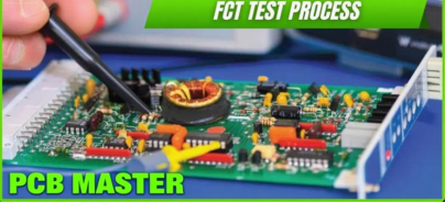
II. FCT Testing (Functional Test)
1.Definition and Core Function
FCT testing is a testing technology that, after PCBA assembly, detects whether the overall function meets design requirements by simulating its actual working environment and input signals. It focuses on "whether the PCBA can achieve preset functions," such as whether a sensor outputs correct signals, whether a chip executes instructions, or whether a display works normally. It is a key link to verify the final usability of products.
Testing Principle and Process
·Testing Principle: Connect the PCBA to a simulated working circuit (e.g., power supply, signal generator, load), send control signals through upper computer software or dedicated test equipment, collect the PCBA's output responses (e.g., voltage, current, waveform, data), and compare them with preset functional standards to determine qualification.
·Test Fixture Design: Design fixtures according to the PCBA's interfaces (e.g., USB, HDMI, power interfaces) to ensure stable connection with external devices during testing.
·Test Program Writing: Write test scripts simulating actual working scenarios, such as sending pairing commands to Bluetooth modules or forward/reverse signals to motor driver boards.
·Environment Setup: Provide the PCBA with a rated power supply and input signals (e.g., audio signals, radio frequency signals), and connect output detection equipment (e.g., oscilloscopes, multimeters, cameras).
·Function Verification: The equipment automatically executes test steps (e.g., power-on self-test, signal transmission, load operation) and records output results (e.g., "Bluetooth connection successful," "Motor speed meets standards").
·Comprehensive Judgment: Mark unqualified functional items (e.g., "No audio output," "Screen flickering") as defects, requiring manual investigation of hardware or software issues.
Advantages and Limitations
Advantages:
·Directly verifies the actual functional performance of the PCBA, which is closely related to user experience.
·Does not rely on test points, making it suitable for high-density PCBs without exposed test points.
·Can detect systematic defects (e.g., circuit design errors, software program vulnerabilities).
Limitations:
·Long test time (complex PCBs may require several minutes), with lower efficiency than ICT.
·High requirements for test environments and fixtures (e.g., radio frequency testing requires shielded rooms), resulting in higher costs.
·Difficult defect localization; if functional abnormalities occur, it is necessary to combine ICT or manual inspection to identify specific causes (e.g., component issues or circuit issues).
III. Core Differences Between ICT and FCT
Comparison Dimension | ICT Testing | FCT Testing |
Test Object | Individual components and circuit connections | Overall functional logic of the PCBA |
Dependent Conditions | Requires pre-reserved test points on PCB and bed-of-nails fixtures | Requires simulated working environment and interface fixtures |
Detection Content | Component parameters (resistance, capacitance, etc.) and continuity | Functional responses (signal output, instruction execution, etc.) |
Defect Types | Assembly defects (wrong components, cold solder joints) and parameter abnormalities | Functional failures (inability to achieve design goals) |
Test Cost | High fixture cost, low per-unit test cost | High fixture and environment costs, high per-unit test cost |
Applicable Stage | Pilot and mass production (early defect interception) | Late mass production and pre-delivery (final function verification) |
IV. Synergistic Effect of ICT and FCT
In electronic manufacturing, ICT and FCT usually form a "complementary test chain":
·ICT takes the lead: By accurately detecting component and circuit defects, it reduces FCT failures caused by basic electrical issues, lowering the difficulty of FCT troubleshooting (e.g., avoiding abnormal chip power supply in FCT due to incorrect resistor installation).
·FCT follows up: After ICT ensures basic electrical normality, functional testing verifies overall usability, ensuring products work properly when delivered to users.
·Joint defect localization: If FCT detects functional abnormalities, ICT can recheck component parameters of related circuits to quickly narrow down fault ranges (e.g., if a sensor has no output in FCT, ICT can detect whether the sensor's power supply resistor is normal).
ICT and FCT are the "front and rear checkpoints" in PCBA quality control: ICT focuses on "basic electrical health," using data-driven methods to intercept hidden assembly defects; FCT focuses on "actual functional compliance," simulating real scenarios to verify product usability. Their combination ensures production efficiency while minimizing the risk of defective products being shipped, making them an indispensable testing technology combination in electronic manufacturing.
Conclusion
In summary, as the core link in electronic manufacturing that transforms "bare boards" into "functional modules," PCB Assembly covers key steps such as incoming inspection, solder paste printing, component assembly (SMT, THT, bonding, Press-Fit, etc.), multi-dimensional testing (AOI, SPI, ICT, FCT, etc.), rework, and final packaging. Each step relies on standardized operations, precision equipment, and strict quality control systems to jointly ensure the reliability and stability of electronic components.
In terms of technical application, SMT and THT are not substitutes but complement each other based on component characteristics (e.g., power, size, reliability requirements). The "hybrid assembly" model has become mainstream in modern electronic manufacturing. Detection technology has evolved from traditional manual sampling to automated, intelligent full-process monitoring (e.g., 3D SPI, AI-driven AOI), enabling precise defect interception and continuous process optimization.
Through systematic specifications (e.g., IQC's "three-document comparison," "risk classification," regular equipment calibration, and full data traceability), PCBMASTER has built a quality assurance loop from source to end, meeting diverse needs in fields such as consumer electronics, automotive electronics, and medical devices, while providing a replicable model for the standardization and efficiency of the electronic manufacturing industry. In the future, as components become more miniaturized and high-density, PCB Assembly will further develop toward higher precision, intelligence, and greenization (e.g., lead-free processes), continuously driving technological upgrading and quality improvement in the electronics industry.
Why choose PCBMASTER: https://www.pcbmaster.com/why
Join us: https://www.pcbmaster.com/login