


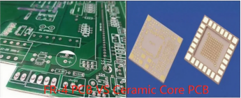
The Heat Dissipation Revolution Ceramic Core PCB Hidden Inside Circuit Boards
Open up the latest 5G smartphone or a Tesla electric control system, and you’ll find a light brown “ceramic piece” hidden in the core layer of the circuit board. It feels cool and hard to the touch, yet it can boost chip performance by 3 times—this isn’t sci-fi, it’s the Ceramic Core PCB, a silent material revolution happening in the electronics industry. Thanks to advanced PCB technology, high-performance ceramic core PCBs are now possible, utilizing specialized substrate materials, insulating materials, and multiple ceramic layers to achieve superior reliability and thermal management.
Traditional FR-4's Dilemma: When the Circuit Board Wears a "Leather Jacket"

Imagine making a sprinter race wearing a leather jacket—that’s the predicament of traditional FR-4 substrates (glass fiber epoxy resin) in high-power devices. Compared to traditional PCBs, ceramic core PCBs offer far superior thermal conductivity and electrical insulation, making them ideal for demanding applications.
·Heat Dissipation Nightmare: Thermal conductivity is only 0.3 W/(m·K), causing chip temperatures to soar (lifespan shortens by 60% at 150℃). This limitation is common to traditional materials and traditional boards, which struggle with effective heat dissipation and long-term reliability.
·Signal Distortion: In the 5G millimeter-wave band, signals attenuate by 0.8dB every inch transmitted
·Environmental Fragility: Delaminates and cracks during -40℃ cold starts; copper traces corrode and fall off in salt spray environments
These pain points plague new energy vehicles, 5G base stations, and aerospace equipment. The solution? Ceramic Core PCBs, which outperform traditional PCBs in thermal management, electrical performance, and durability.
The Birth of Ceramic Core PCBs: Transformation from Powder to Precision Carrier
Step One: Choosing the “Ceramic Gene”Just like building a house starts with the foundation, the ceramic base material determines the performance ceiling:
·The Common Soldier - Alumina (Al₂O₃): Thermal conductivity 20-30W/(m·K), cost-effective, preferred for home appliance control boards. Alumina PCBs are widely used in low to medium power devices due to their affordability and good electrical insulation.
·The Heat Dissipation King - Aluminum Nitride (AlN): Thermal conductivity 180-230W/(m·K), the “superconducting heat sink” for new energy vehicle electric controls
·The Hardcore Performer - Silicon Carbide (SiC): Temperature resistance >1000℃, hardness comparable to diamond, dedicated for satellite antennas
Step Two: Forming the “Ceramic Biscuit”Transforming ceramic powder into thin sheets, two processes shine:
·Dry Pressing: Like pressing mooncakes, 10-30MPa pressure forms green bodies, suitable for low-cost mass production
·Tape Casting: Spreading ceramic slurry into 0.1mm thin sheets (thinner than a credit card), thickness tolerance for 5G base station boards is only ±5μm
Step Three: The High-Temperature “Ceramic Purgatory”Green bodies must endure the fiery test:
**·**Alumina sinters at 1600℃, Aluminum Nitride requires 1800℃ (temperature difference < ±5℃)
**·**Cooling must be “slow cooling,” otherwise thermal stress will make the substrate crack like glass
Step Four: Putting on the “Metal Conductive Coat”
·Thick Film Process: Screen printing silver/copper “conductive ink,” sintered at 800℃ to form circuits—low cost, suitable for motor electrodes
·Thin Film Process: Magnetron sputtering nano metal layers, photolithography etching to create 50μm fine lines (finer than a human hair)—standard for 5G RF modules
Key Breakthrough DPC Process: Vacuum sputtering + electroplated copper, achieving 0.05mm line accuracy, essential for LEDs and chip packaging
Comparison Table: Ceramic Core PCB vs. Traditional PCB vs. Metal Core PCB
Feature | Ceramic Core PCB | Traditional PCB (FR-4) | Metal Core PCB |
Thermal Conductivity | High (20-230 W/m·K) | Low (0.3 W/m·K) | Medium-High (1-8 W/m·K) |
Electrical Insulation | Excellent | Good | Moderate |
Heat Resistance | Excellent | Limited | Good |
Fabrication Complexity | High | Low | Medium |
Typical Materials | Alumina, AlN, SiC | FR-4, CEM | Aluminum, Copper |
Applications | High-power, RF, LED | Consumer electronics | Power LEDs, automotive |
Note: Metal core PCBs use a metal base (aluminum or copper) to improve heat dissipation, making them suitable for high-power and high-temperature applications. However, ceramic core PCBs offer even higher thermal conductivity and better electrical insulation, making them preferable for the most demanding environments.
In summary, the ceramic circuit board stands out as a superior alternative to traditional PCBs and metal core PCBs, especially where high thermal conductivity, electrical performance, and reliability are critical.
Ceramic PCB Core vs. FR-4: Ultimate Showdown in Six Dimensions
Comparison Item | Ceramic Core PCB | Traditional FR-4 |
Thermal Conductivity | AlN substrate 230W/(m·K) (566 times FR-4) | 0.3-0.4W/(m·K) Chips "wrapped in a quilt" |
Insulation Strength | Breakdown voltage ≥20KV/mm (10 times FR-4) | Requires additional insulation layers |
High-Frequency Perf. | Dielectric loss Df <0.001 (5G signal zero distortion) | Df >0.025 (severe attenuation in mmWave) |
Cost & Lead Time | Prototyping costs thousands, lead time 10-15 days | Prototyping costs hundreds, 24-hour delivery |
Process Complexity | DPC/HTCC etc. 10+ processes, laser drilling ±25μm | Mature assembly line, mechanical drilling ≥0.1mm |
Extreme Env. Survival | -55℃~850℃ no cracking, resistant to salt spray/radiation | >100℃ temp. diff. causes delamination, fails in damp heat |
Inside the Revolution: How Ceramic Core PCBs Are Made
Beneath the surface of every high-performance device lies a marvel of engineering: the ceramic core PCB. The journey from raw ceramic powder to a finished ceramic printed circuit board is a story of precision, innovation, and the relentless pursuit of better thermal performance.
It all begins with the right ceramic material. The foundation of every ceramic PCB is its substrate, typically crafted from advanced materials like aluminum oxide (Al₂O₃), aluminum nitride (AlN), silicon carbide (SiC), or even beryllium oxide (BeO). Each ceramic material brings its own strengths to the table: aluminum oxide boards are cost-effective and offer good thermal conductivity, while aluminum nitride boards are prized for their extremely high thermal conductivity—making them the go-to choice for power electronics and LED lighting. Silicon carbide and beryllium oxide push the envelope further, delivering excellent thermal conductivity and electrical insulation for the most demanding high temperature applications.
The manufacturing process starts with transforming these ceramic powders into a robust substrate. The powders are mixed with binders and solvents to form a uniform slurry, which is then shaped into thin layers using techniques like tape casting or injection molding. This step is crucial for achieving the precise thickness and flatness required for modern electronics. Once shaped, the ceramic “green body” is carefully dried and then sintered at high temperatures—sometimes exceeding 1800°C for aluminum nitride. This sintering process not only removes the binders but also fuses the ceramic particles together, creating a dense, mechanically strong ceramic substrate with a low coefficient of thermal expansion.
Next comes the creation of the conductor layers—the nervous system of the ceramic PCB. Depending on the application, manufacturers use either thick film or thin film techniques. Thick film ceramic PCBs are made by screen printing conductive pastes—often containing silver, gold, or copper—directly onto the ceramic substrate. These pastes are then fired at high temperatures, bonding the metal to the ceramic and forming durable circuit traces. For applications demanding finer features and higher connection density, thin film ceramic PCBs use advanced methods like vacuum deposition or sputtering to lay down ultra-thin metal layers, which are then patterned using photolithography or laser ablation.
Precision is key at every stage. Via holes are laser-drilled to connect different layers, and solder masks are applied to protect the circuit traces. Surface mount technology (SMT) components are then attached, taking full advantage of the ceramic board’s ability to withstand high temperatures and provide efficient heat dissipation.
What sets ceramic PCBs apart is their combination of properties: extremely high thermal conductivity for rapid heat removal, excellent electrical insulation to prevent short circuits, and a low coefficient of thermal expansion that minimizes stress during temperature swings. This makes ceramic printed circuit boards the backbone of power electronics, automotive electronics, and high-brightness LED lighting—anywhere efficient heat dissipation and reliability are non-negotiable.
Advanced materials like gold conductive pastes and beryllium oxide substrates push performance even further, enabling ceramic PCBs to thrive in the harshest environments, from under the hood of electric vehicles to the vacuum of space.
As the electronics industry demands ever more power in ever smaller packages, the manufacturing process of ceramic core PCBs continues to evolve. With their unmatched blend of thermal, electrical, and mechanical properties, ceramic PCBs are not just keeping up—they’re leading the revolution from the inside out.
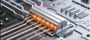
Innovative Applications with High Thermal Conductivity
1. The “Life-Saving Ceramic” for New Energy VehiclesIn 800V high-voltage platforms, ceramic-filled substrates control the temperature rise of electric control modules to within 12℃ (traditional solutions >30℃). More crucially for 77GHz radar—ceramic substrates ensure precise detection in snowy conditions with ±0.05 dielectric constant stability. The use of thick film ceramic PCBs in automotive power electronics also allows for the integration of electric capacitors, improving reliability and performance in demanding environments.
2. The “Signal Guardian” for 5G Base StationsHybrid lamination becomes a cost-saving marvel: embedding ceramic only in the signal layers of a 12-layer board, while keeping the power layers as FR-4, reduces costs by 22% while decreasing 28GHz signal loss by 18%. In these advanced multilayer ceramic boards, passive components can be embedded within the inner layers, increasing component and connection density and enhancing thermal management. Ceramic PCBs are also highly suitable for microwave circuits in 5G and satellite applications due to their stability and reliability.
3. The “Slimming Expert” for LEO SatellitesA 6-layer ceramic HDI board achieves 40GHz signal transmission, compresses antenna thickness to 1.2mm, and reduces overall satellite weight by 40%—saving $200,000 in annual fuel per satellite. This is made possible by the high component and connection density enabled by the superior properties of ceramic PCBs.
The Future Battle: Chinese Manufacturing Breaks Japanese Monopoly
Global production capacity is drastically changing:
·Asia-Pacific accounts for 90% of global capacity: Mainland China 44.42%, Taiwan region 42.76%
**·**Fujian Huaqing’s AlN substrates break Japan’s Maruwa monopoly **·**Lieban PCB’s BaTiO₃ nano-ceramic substrate passed AEC-Q200 certification, cost 25% lower than imports
Green Manufacturing Breakthroughs Simultaneously:
**·**Etchant regeneration technology achieves copper recovery rate >90%, reducing wastewater by 60%. Green manufacturing also focuses on the recovery and recycling of metal cores and metal core PCBs, supporting sustainable production practices.
**·**Halogen-free base materials comply with EU carbon tariffs, carbon footprint reduced by 18% annually
Conclusion: The "Wall-Breaker" of Foundational Materials
While the world focuses on the computing marvels of ChatGPT, few notice—powering the operation of trillion-parameter large models are those ceramic-cold-glow substrates deep inside servers. Born from 1800℃ flames, they carry the era's computing power with nanometer precision, silently rewriting the performance limits of electronic devices.
Ceramic Core PCB Value Formula:
Heat Dissipation Efficiency × Signal Fidelity ÷ Environmental Losses = Ultimate Reliability of Electronic Devices
FAQs

Q. What is the biggest advantage of ceramic core PCB compared to traditional FR-4 PCB?
A. The biggest advantage of ceramic core PCBs lies in their exceptional thermal conductivity. FR-4 PCBs typically have a thermal conductivity of only 0.2 - 0.4 W/m·K, while ceramic core PCBs, such as those with alumina cores, can achieve 20 - 30 W/m·K, and aluminum nitride cores can reach 170 - 200 W/m·K—tens or even hundreds of times that of FR-4. This allows ceramic core PCBs to dissipate heat much more efficiently in high-power electronic devices, preventing performance degradation and component damage due to overheating, significantly improving device reliability and stability. Additionally, the coefficient of thermal expansion (CTE) of ceramic core PCBs better matches that of metals, resulting in lower thermal stress during temperature changes, reducing issues like solder joint cracking and trace breakage, further enhancing product lifespan. Advanced substrate materials used in ceramic core PCBs also provide superior electrical properties, such as high-frequency stability and signal integrity, making them ideal for demanding applications.
Q. Which electronic devices are ceramic core PCBs suitable for?
A. Ceramic core PCBs are suitable for various electronic devices with high demands for heat dissipation and reliability. In power electronics, such as battery management systems for electric vehicles, charging piles, and inverters, these devices generate significant heat during operation, and the high thermal conductivity of ceramic core PCBs effectively dissipates this heat, ensuring power devices function properly. In the communication field, high-frequency devices like 5G base stations and satellite communication equipment require PCBs with good electrical performance and heat dissipation; ceramic core PCBs meet these requirements, reducing signal transmission loss. In aerospace and military equipment, where environmental conditions are harsh, demanding high mechanical strength, temperature resistance, radiation resistance, etc., ceramic core PCBs, with their excellent overall performance, are the ideal choice. Furthermore, high-brightness LED lighting fixtures often use ceramic core PCBs to solve the heat dissipation problem of LED chips, improving the luminous efficiency and lifespan of the fixtures. Ceramic PCBs offer unique benefits for high-reliability and high-performance devices, especially in industries where both thermal and electrical properties are critical.
Q. Is the manufacturing process of ceramic core PCB complex?
A. The manufacturing process of ceramic core PCBs is relatively complex. First is the preparation of the ceramic substrate, which requires high-purity ceramic powders like aluminum nitride or alumina. This involves multiple steps: mixing, forming, debinding, and sintering, to obtain a ceramic substrate with the required strength and performance. The sintering process requires precise temperature and atmosphere control to ensure the density and properties of the ceramic substrate meet specifications. Then comes circuit fabrication on the ceramic substrate, involving drilling, metallization, circuit patterning, and other processes. Due to the high hardness and brittleness of ceramic materials, drilling usually employs laser drilling technology to ensure hole precision and quality. Metallization processes include various methods like Direct Bonded Copper (DBC), Active Metal Brazing (AMB), etc. Each has its characteristics and applications, requiring strict control of process parameters. Selecting the right substrate material is crucial for achieving the desired thermal and electrical performance in the final product. Finally, processes like circuit pattern creation, plating, etching, and surface treatment are needed. Each step requires strict control to produce high-quality ceramic core PCBs.
Q. Why is the cost of ceramic core PCB higher than traditional FR-4 PCB?
A. The high cost of ceramic core PCBs is mainly due to several reasons: First, raw material costs are high. The ceramic powders used, such as high-purity aluminum nitride or alumina, are expensive and require strict impurity content and particle size specifications. Second, the manufacturing process is complex. Each step, from ceramic substrate preparation to circuit fabrication, requires high-precision equipment and strict process control—like laser drilling, high-temperature sintering, precise metallization processes—all increasing production costs. Third, production efficiency is relatively lower. Due to the complex process, the production cycle is longer, limiting output per unit time, thus increasing the cost allocated per product. Fourth, quality inspection costs are high. To ensure the quality and reliability of ceramic core PCBs, multiple stringent tests are necessary, such as thermal performance testing, electrical performance testing, and mechanical performance testing, further raising costs.
Q. What issues should be noted when using ceramic core PCBs?
A. When using ceramic core PCBs, attention should be paid to thermal stress issues. Since there is still some difference in the coefficient of thermal expansion (CTE) between ceramic and metal, significant temperature changes during use can generate thermal stress, leading to solder joint cracking or trace damage. Therefore, avoid rapid temperature changes or take measures to mitigate thermal stress, such as using stress-buffering materials. Regarding mechanical stress, although ceramic core PCBs have good mechanical strength, avoid severe impact and vibration during installation and use to prevent the ceramic substrate from cracking. Also, note the solderability of ceramic core PCBs. The surface properties of some ceramic materials may affect soldering effectiveness; choose appropriate soldering processes and materials to ensure good solder joint quality. Additionally, when designing circuits, fully consider the characteristics of ceramic core PCBs, reasonably layout components, and optimize trace design to achieve their best performance. Advancements in ceramic PCB technology benefit PCB designers by enabling more robust and reliable circuit layouts, especially for applications requiring high thermal and electrical performance.
Why PCBMASTER: https://www.pcbmaster.com/why
Join US:https://www.pcbmaster.com/login

