








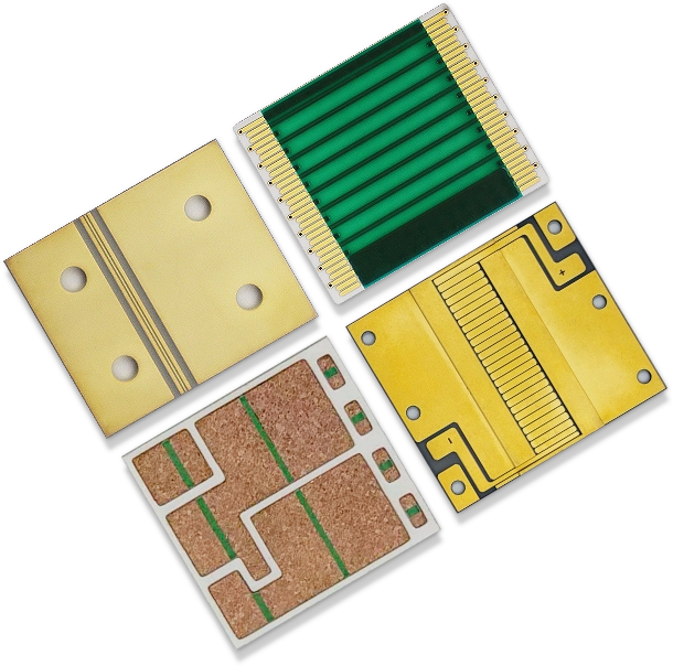
セラミック基板 製品シリーズ
多様なシナリオニーズに合わせて、パフォーマンス、信頼性、コスト効率のバランスを最適化した材料ソリューションを提供します。
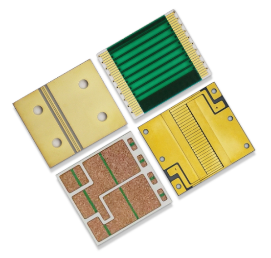
当社が生産するセラミックPCB材料には以下が含まれます アルミナ、窒化アルミニウム、窒化ケイ素、酸化ベリリウム(BeO)、サファイア、ガラス、フェライト、ダイヤモン.
高純度アルミナ(≥96% Al₂O₃)、優れた電気絶縁性と熱伝導性を備え、中電力電子機器に最適です。
.webp)
優れた熱伝導性と一致した熱膨張率、高電力高信頼性アプリケーション向けに設計。
.webp)
窒化アルミニウム(AlN)
優れた耐高温性、耐食性、耐放射線性、航空宇宙と高エネルギー環境向けに設計。
.webp)
ZTAセラミック基板はジルコニア強化アルミナ材料で、靭性が向上し、バランスの取れた性能(高強度、高硬度、耐衝撃性)と耐高温性、耐食性を備えています。
.webp)
ジルコニア強化アルミナ(ZTA)
材料特性比較
| 材料 | 熱伝導率 | 絶縁性 | 靭性 | コスト |
|---|---|---|---|---|
| アルミナ(Al₂O₃) |
低電力デバイスに十分
|
優れた電気絶縁性
|
脆性があり、欠けやすい
|
低い
生産プロセスが成熟
|
| 窒化アルミニウム(AlN) |
優れた放熱性
|
大部分の電子機器に適合
|
窒化ケイ素より低い
|
中~高
原材料コストが高い
|
| 窒化ケイ素(Si₃N₄) |
焼結プロセスに依存
|
構造用途に十分
|
最も高い耐破壊性
|
高
製造プロセスが複雑
|
コア 技術優位性
材料選定からプロセス管理まで、あらゆる細部が「高信頼性」基準に基づき、業界トップクラスのセラミック基板を製造します。
卓越した熱伝導性
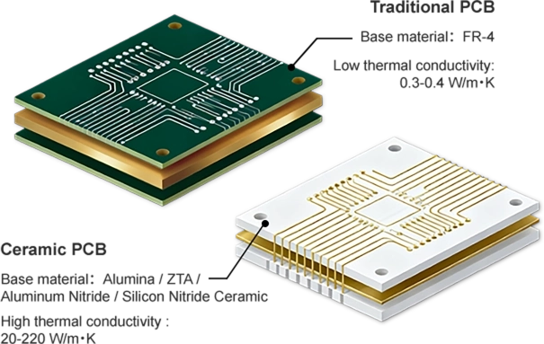
基板の熱伝導率は最大220 W/(m·K)に達し、従来のFR-4の500~600倍です。部品の動作温度を低下させ、寿命を延長します。
極端な温度耐性
-55℃~1500℃の極端な温度範囲で安定動作し、航空宇宙・軍事産業の高耐熱性に対する厳しい要求を満たします。
高精度回路
先進的な加工技術により、0.05mmの超微細配線と0.1mmのマイクロビアを実現し、高気密性、低アウトガス、高周波・高速信号伝送のニーズに応えます。
CTE整合設計
熱膨張係数(CTE)が3ppm/℃でチップと一致し、はんだ接合部の熱応力を効果的に低減し、製品の信頼性を向上させます。
全工程品質管理
AS9100、IATF16949規格に準拠し、熱衝撃試験を実施しており、不良率を0.03%以下に制御しています。
オーダーメイドソリューション
材料選定、構造設計、SMT実装、ICパッケージング、熱シミュレーションまでのワンストップサービスを提供し、特定のシナリオにおけるパフォーマンスとコストを最適化します。
従来PCB vs セラミック基板
セラミック基板は熱伝導性、耐熱性、信頼性に大幅な優位性があり、高電力・高信頼性用途に最適です。
- 放熱能力 +600%
- 拡張された使用温度範囲
- 寿命 +3~10倍
- 電力密度 +2~10倍
精度 製造能力
「ミリメートル級精度、マイクロメートル級制御」を基準とし、5つのコアプロセスを通じて高品質を保証します。
応用分野
新エネルギー自動車から医療機器、5G通信から航空宇宙まで、当社のセラミック基板ソリューションはハイエンド分野のコア選択肢です。
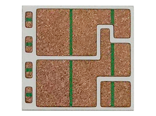
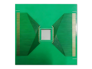
99%アルミナセラミックPCB
- 素材: 99%アルミナセラミックPCB
- 層数: 2層
- 厚さ: 1.00mm
- トラック/スペーシング: 8mil
- 表面処理: OSP
- 特殊技術: 高純度99%アルミナセラミック;穴充填の高平坦性
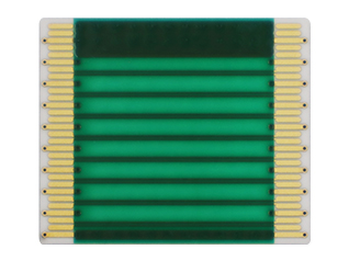
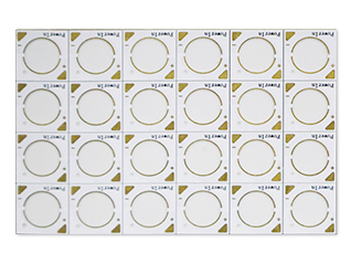
Zr 強化 Al₂O₃PCB(ZTAPCB)
- 素材: ジルコニア強化アルミナ(ZTA)
- 層数: 2層
- 厚さ: 1.50mm
- トラック/スペーシング: 4/4mil
- 表面処理: 無電解金めっき
- 特殊技術: インピーダンス制御±7%
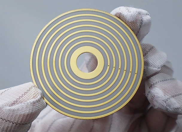
AlN セラミック PCB
- 素材: 窒化アルミニウムセラミック
- 層数: 2層
- 厚さ: 0.8mm
- トラック/スペーシング: 4/4mil
- 表面処理: 窒化アルミニウムセラミック基材
- 特殊技術: 狭配線スペース。寸法精度。ICボンディング対応
代表的な顧客事例
ポータブルMRI装置のRFモジュールの電力密度が20W/cm³に増加したため、従来のFR4基板(熱伝導率0.3W/m·K)ではチップ接合温度が150℃に達し、熱膨張不整合によりはんだ接合部がクラックする結果となります。
- 材料革新: 熱伝導率170W/m·K(FR4の567倍)、熱膨張係数(CTE)4.5ppm/℃の窒化アルミニウム(AlN)基板を採用。シリコンチップ(3ppm/℃)との高い整合性により、熱ミスマッチ問題を根本的に解決します。
- プロセス最適化: 直接銅接合(DBC)プロセスによりセラミックと銅層の冶金的接合を実現し、界面熱抵抗 < 0.5℃·cm²/W。銅ピラーアレイ設計と組み合わせて垂直熱伝導チャネルを形成し、総熱抵抗を0.15℃/Wに低減します。
- 信頼性保証: 活性金属ろう付け(AMB)を使用して耐熱衝撃性を強化。-55℃~150℃で1000サイクルの試験後、はんだ接合強度維持率は> 95%です。
- 結果: チップ接合温度は85℃に低下し、電力密度は22W/cm³に達します。製品はISO 13485医療認証を取得し、デバイスの10年寿命要件を満たしています。
ブログ&ニュース
-
 Aluminum Oxide vs. Aluminum Nitride for Ceramic PCBs: How to Choose?Ceramic PCBs are essential components in modern electronics, offering superior performance in high-temperature, high-power, and high-frequency applications. These PCBs are made from ceramic materials, which provide better heat dissipation, ...Jan 22, 2026もっと見る
 -
Aluminum Nitride Ceramic PCBs: Benefits, Applications, and TrendsAs electronics get smaller and more powerful, managing heat and maintaining electrical insulation are increasingly critical. Traditional materials often can't meet these rising demands. Aluminum Nitride (AlN) ceramic PCBs offer a breakthrou...Jan 13, 2026もっと見る
-
Ceramic PCBs: Key Features and ApplicationsCeramic PCBs are transforming the electronics industry by delivering exceptional performance in extreme conditions. Unlike traditional FR4 PCBs, which use organic materials, ceramic PCBs are crafted from advanced ceramics like alumina, alum...Dec 11, 2025もっと見る
-
How Ceramic PCBs Enhance Electronics: Key Materials & Manufacturing Processes ExplainedAs electronics continue to evolve, particularly in high-power and high-temperature environments, traditional PCB (Printed Circuit Board) materials are starting to show their limitations. To meet the increasing demands for superior thermal m...Dec 11, 2025もっと見る
よくある質問 セラミックPCBについて
その他の質問がありますか?弊社の技術チームが支援の準備ができています。
Customer Reviews
Authentic feedback from clients, validating our product quality and service level.
"Our industrial power modules operate long-term in high-temperature environments above 150℃. Previously, using ordinary PCBs led to frequent thermal failures. After switching to ceramic-based PCBs, the thermal conductivity efficiency has significantly improved. They've run continuously for 6 months with zero failures, and the device temperature has dropped by 28℃ compared to before. The stability has completely exceeded expectations—truly a reliable choice for high-power applications!"
—— Mark Reynolds, Senior Power Electronics Engineer
"The core heat dissipation area of our high-end projectors has long been limited by space constraints. The thin and lightweight properties of ceramic-based PCBs perfectly fit the product design: despite a thickness of only 0.6mm, they quickly conduct heat away from the chip. This allows the projector to operate continuously for 3 hours while keeping the body temperature below 45℃. User feedback indicates a significant improvement in experience, with the repair rate dropping by 35%."
—— Emily Carter, RF Systems Engineer
"When selecting a substrate for our automotive radar module, we compared multiple options and ultimately chose ceramic-based PCBs. Not only can they withstand vibration and impact during vehicle operation, but signal transmission remains stable within the wide temperature range of -40℃ to 125℃. After 1,000 thermal cycle tests, there was no cracking or desoldering whatsoever—fully meeting automotive-grade reliability requirements."
—— David Larson, R&D Electrical Engineer

