


Reflow Soldering Explained: How the SMT Reflow Process Works in PCB Manufacturing
In modern electronics manufacturing, product performance is increasingly defined by precision at the microscopic level. As components continue to shrink and circuit density increases, the way electrical connections are formed on a PCB has become a critical factor in overall reliability.
Among the various assembly techniques used in PCB production, one process stands out as the backbone of high-volume surface mount manufacturing: reflow soldering. It enables consistent, automated, and highly controlled formation of solder joints, making it essential for today’s SMT-based production lines.
However, while the concept may seem straightforward, the actual process behind it involves carefully engineered thermal stages, tightly controlled parameters, and precise coordination between multiple manufacturing steps.
To fully understand how reliable solder joints are formed—and why this method dominates modern PCB assembly—it is necessary to look closely at how the SMT reflow process actually works, step by step, and what factors influence its performance in real manufacturing environments.
What is reflow soldering in SMT PCB manufacturing and why is it essential?
Reflow soldering in SMT PCB manufacturing is a controlled heating process that melts solder paste to permanently form electrical and mechanical connections between surface-mounted components and a PCB, and it is essential because it enables precise, reliable, and high-volume assembly of modern high-density electronic devices.
Definition of reflow soldering in surface mount technology (SMT)
Reflow soldering is a PCB assembly process where solder paste is heated until it melts, then cooled to form strong electrical and mechanical connections between components and the board.
Reflow soldering in SMT (Surface Mount Technology) refers to the method of attaching electronic components directly onto the surface of a PCB using solder paste. The solder paste is a mixture of tiny solder particles and flux, printed onto specific pads on the board.
When the PCB passes through a reflow oven, the temperature rises in a controlled way. First, the solder paste becomes soft and activates the flux. Then, at higher temperature, the solder melts and “flows” around the component leads and pads. Finally, as the board cools down, the solder solidifies and locks the component in place.
This controlled heating process creates both an electrical path and a strong mechanical bond at the same time. For example, in a smartphone motherboard, thousands of tiny components are held in place only by these solder joints, yet they must survive drops, heat, and long-term use.
In simple terms, reflow soldering is like “controlled melting and freezing” of solder to glue and connect electronic parts with high precision.
Why reflow soldering is the dominant process in modern PCB assembly
Reflow soldering is widely used because it supports very small components and works well with high-density, high-performance PCB designs.
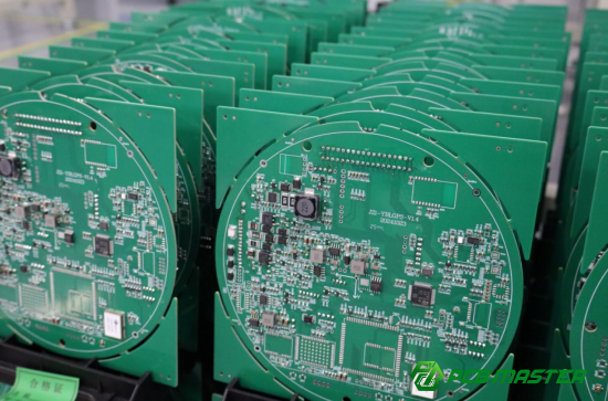
Modern electronics such as smartphones, laptops, and automotive control units require extremely small and tightly packed components. Reflow soldering is ideal because it can handle micro-sized parts like 0201 resistors or fine-pitch ICs without manual soldering.
Another reason it dominates PCB assembly is its compatibility with HDI (High-Density Interconnect) and multilayer boards. These boards have complex routing and limited space, so traditional soldering methods cannot achieve the same precision or consistency.
For example, in an automotive ECU (Engine Control Unit), hundreds of components must be placed with exact alignment. Reflow soldering ensures every joint is formed under identical temperature conditions, reducing human error and improving reliability.
Compared with hand soldering, reflow soldering is also far more scalable. Once the process is set, thousands of boards can be produced with nearly identical quality, which is critical for mass production environments.
Where reflow soldering fits in the SMT assembly workflow
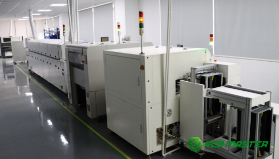
Reflow soldering happens after component placement and before inspection in the SMT production line, acting as the key step that permanently forms all solder joints.
In a typical SMT (Surface Mount Technology) production line, the workflow follows a clear sequence:
1. Solder paste printing: A stencil printer applies solder paste onto PCB pads.
2. Component placement: A pick-and-place machine positions components onto the pasted pads.
3. Reflow soldering (core process): The PCB enters a reflow oven where controlled heating melts the solder and forms permanent joints.
4. Inspection: The finished board is checked using AOI (Automated Optical Inspection) or X-ray systems.
For example, in a consumer electronics factory, a PCB may travel on a conveyor system through each stage automatically. The reflow oven acts as the “bonding stage,” where all previously placed components are permanently fixed in one continuous thermal cycle.
This position in the workflow is critical because any error before reflow (such as misaligned components or uneven solder paste) will become permanent after the heating cycle. That is why upstream process control is essential for successful SMT reflow soldering results.
How does the reflow soldering process work step by step in PCB manufacturing?
The reflow soldering process in PCB manufacturing works by printing solder paste, placing components, and then passing the board through a controlled multi-stage heating cycle (preheat, soak, peak reflow, and cooling) that melts and solidifies the solder to form reliable electrical and mechanical connections.
Step 1 — Solder paste printing on PCB pads
Solder paste printing is the process of applying a precise amount of solder paste onto PCB pads using a stencil before components are placed.
In SMT reflow soldering, the process starts with solder paste printing in PCB manufacturing, where a stainless-steel stencil is aligned over the PCB. A squeegee blade then spreads solder paste across the stencil openings so it deposits only on the required pads.
The key factor here is paste deposition control in PCB assembly. If too much solder paste is applied, it can cause solder bridges after reflow. If too little is applied, the joint may become weak or fail electrically.
For example, in smartphone PCB production, even a 0.1 mm variation in paste volume can affect signal stability. That is why factories tightly control stencil thickness, paste viscosity, and printing pressure.
Step 2 — SMT component placement before reflow
Component placement is the process where machines accurately position electronic parts onto solder-pasted pads before heating.
After printing, a pick-and-place machine in SMT assembly places components directly onto the solder paste. These machines use vacuum nozzles and vision systems to achieve extremely high precision.
The most important requirement is placement accuracy in PCB manufacturing, especially for fine-pitch ICs and micro components. Even a small offset can cause poor solder joints or short circuits after reflow.
For example, in an HDI PCB used in a laptop motherboard, components are placed with micron-level accuracy so they perfectly align with solder paste deposits. The sticky nature of solder paste helps hold components temporarily before they enter the oven.
Step 3 — Preheat zone in reflow oven
The preheat zone gradually increases PCB temperature to prevent thermal shock and prepare solder paste for reflow.
In the reflow soldering preheat stage, the PCB enters a controlled heating zone where temperature rises slowly. This is important to avoid thermal shock in PCB components, which can crack sensitive parts.
During this stage, the flux inside the solder paste begins to activate, and solvents start to evaporate. This helps clean oxidation from metal surfaces and prepares them for strong bonding later.
For example, if a PCB is heated too quickly (like placing it directly into high heat), ceramic capacitors may crack. That is why reflow ovens use a controlled ramp-up profile.
Step 4 — Soak zone for thermal stabilization
The soak zone ensures the entire PCB reaches a uniform temperature and activates flux for better soldering quality.
In the soak phase of reflow soldering, the PCB temperature is held steady for a short time. This allows different areas of the board—thick and thin sections—to equalize in temperature.
This step is important for thermal balance in PCB reflow process, especially for large multilayer boards where heat spreads unevenly.
At the same time, the flux becomes fully active and removes oxidation from copper pads and component leads, improving solder wetting during the next stage.
For example, in automotive PCBs, soak control is critical because uneven heating can lead to unreliable solder joints under vibration conditions.
Step 5 — Reflow (peak temperature zone)
The reflow zone is where solder melts, flows, and forms strong electrical and mechanical connections.
During the peak reflow stage in SMT soldering, the temperature reaches the melting point of solder (typically 217°C–245°C for lead-free solder). The solder paste becomes liquid and flows around pads and component leads.
This process creates solder wetting in PCB assembly, where molten solder spreads evenly and forms a strong bond.
At this stage, intermetallic compounds (IMC) formation in solder joints occurs. These IMCs are essential because they create a strong metallurgical connection between copper and solder.
For example, in a fine-pitch QFN chip, proper peak temperature ensures all pins form uniform joints without voids or weak connections.
Step 6 — Cooling zone and solidification
The cooling zone solidifies solder joints in a controlled way to ensure strength and prevent defects.
In the cooling stage of reflow soldering, the PCB temperature is reduced in a controlled manner. This prevents thermal stress and helps solder solidify evenly.
A proper cooling rate is critical for reflow solder joint reliability, because cooling too fast can cause cracks, while cooling too slow can lead to weak grain structures.
For example, in high-reliability aerospace electronics, controlled cooling is used to ensure solder joints can withstand vibration and temperature cycling over long periods.
At the end of this stage, all components are permanently fixed, forming strong electrical paths and mechanically stable joints across the entire PCB.
What is a reflow oven profile and how does it affect soldering quality?
A reflow oven profile is a precisely controlled temperature curve used during PCB reflow soldering, and it affects soldering quality by determining whether solder joints form correctly—ensuring proper melting, wetting, and cooling to avoid defects like cold joints, overheating damage, and weak connections.
Key stages of a standard reflow temperature profile
A reflow oven profile is a controlled temperature curve that guides the PCB through heating and cooling stages to ensure proper solder melting and reliable joint formation.
A reflow soldering temperature profile in PCB manufacturing defines how temperature changes over time inside the reflow oven. It is not random heating—it is a carefully designed curve that ensures stable solder joints.
Ramp-up rate control (°C/sec)
The ramp-up stage gradually increases temperature, usually around 1–3°C per second, to avoid thermal shock. If heating is too fast, sensitive components like ceramic capacitors may crack. In real SMT production lines, engineers carefully tune this rate for different PCB thicknesses.
Soak time optimization
The soak zone holds the temperature steady so the entire PCB becomes uniform. This step is important in SMT reflow soldering profiles because thick and thin areas heat differently. Soak time also activates flux, which removes oxidation from copper pads.
Peak temperature window (lead-free vs. leaded solder)
This is the highest temperature stage where solder melts. For lead-free reflow profiles, peak temperatures are typically 235°C–245°C, while leaded solder is lower, around 210°C–230°C. Staying within this window ensures proper wetting without damaging components.
How temperature profiles impact solder joint reliability
Temperature profiles directly control whether solder joints are strong and defect-free or weak and unreliable.
Cold solder joints caused by insufficient heat
If the reflow oven temperature profile is too low, solder may not fully melt. This creates dull, weak joints called cold solder joints, which can cause intermittent failures in products like smartphones or automotive control boards.
Component damage caused by overheating
If temperature is too high or exposure time is too long, components can be damaged. For example, IC packages may delaminate or plastic housings may warp. This is a common issue in poorly calibrated PCB reflow soldering processes.
In practice, factories run test boards called “thermal profiling coupons” to ensure the oven settings match the product requirements before mass production.
Differences between lead-free and leaded reflow profiles
Lead-free and leaded solder require different temperature profiles because they melt at different temperatures and behave differently during reflow.
Higher melting point requirements for lead-free solder
Lead-free solder (commonly SAC alloys) melts at a higher temperature than traditional leaded solder. This means the lead-free reflow soldering profile must reach higher peak temperatures while still protecting components.
Adjustments in soak and peak zones
Lead-free profiles often require longer soak times and tighter control of the peak zone to ensure proper wetting. Leaded profiles are more forgiving and operate at lower thermal stress levels.
Comparison table
| Feature | Leaded Reflow Profile | Lead-Free Reflow Profile |
| Peak Temperature | ~210–230°C | ~235–245°C |
| Melting Behavior | Lower melting point | Higher melting point |
| Thermal Stress | Lower | Higher |
| Process Window | Wider | Narrower |
| Common Use | Legacy electronics | Modern consumer & industrial electronics |
For example, automotive and aerospace PCBs almost always use lead-free profiles due to environmental regulations, even though they require stricter process control and better thermal management.
What are the most common defects in reflow soldering and how do they occur?
The most common reflow soldering defects include solder bridging, tombstoning, cold solder joints, and voids, and they occur due to issues such as excess or misaligned solder paste, uneven heating, insufficient reflow temperature, and trapped gases during the solder melting and cooling process.
Solder bridging caused by excessive paste or misalignment
Solder bridging happens when too much solder paste or poor component alignment causes two adjacent pads to connect unintentionally.
In reflow soldering defects in PCB assembly, solder bridging is one of the most common issues. It occurs when molten solder flows beyond its intended pad and forms an unwanted electrical connection between two nearby pads.
This usually happens due to excess solder paste printing in SMT process or inaccurate stencil design. It can also occur if components are slightly misaligned during placement, especially in fine-pitch ICs.
For example, in smartphone PCB production, even a tiny excess of paste can cause a bridge between two IC pins, leading to short circuits and device failure.
Tombstoning effect in small passive components
Tombstoning happens when one side of a small component lifts up during reflow due to uneven heating or surface tension imbalance.
The tombstoning defect in reflow soldering is common in small components like resistors and capacitors. During heating, if one pad melts faster than the other, surface tension pulls the component upright like a “tombstone.”
This is usually caused by uneven heat distribution in PCB reflow process or inconsistent solder paste volume on each pad.
For example, in LED circuit boards or wearable devices, tiny 0402 components are highly sensitive to this defect because even small thermal differences can create imbalance.
Cold solder joints due to insufficient reflow temperature
Cold solder joints occur when solder does not fully melt, resulting in weak electrical and mechanical connections.
In cold solder joint defects in SMT reflow soldering, the solder paste does not reach the correct melting temperature or cooling is too fast before proper wetting occurs.
This creates dull, grainy-looking joints that may still look connected but have poor conductivity and low mechanical strength.
For example, in automotive control modules, cold joints can cause intermittent signal loss, especially under vibration or temperature changes.
This defect is often linked to incorrect reflow oven temperature profile settings or insufficient peak temperature control.
Voids in solder joints and their impact on reliability
Voids are trapped gas pockets inside solder joints that reduce strength and heat conductivity.
In reflow soldering void defects in PCB assembly, voids form when flux gases or air cannot escape during the melting stage. These gas pockets become trapped inside the solidified solder joint.
Voids reduce the effective contact area between solder and pad, which weakens both electrical and thermal performance. This is especially critical in high-power devices like LED modules or power electronics.
For example, in power IC packaging, excessive voiding can lead to overheating because heat cannot efficiently transfer through the solder joint.
Void formation is often controlled by optimizing reflow profile soak time, peak temperature, and vacuum-assisted reflow techniques in advanced manufacturing environments.
How to optimize reflow soldering for high-quality PCB assembly results?
Optimizing reflow soldering for high-quality PCB assembly requires controlling solder paste and stencil design, stabilizing oven temperature profiles and conveyor speed, ensuring precise component placement, and using AOI and X-ray inspection to detect and eliminate defects after reflow.
Optimizing solder paste selection and stencil design
Reflow soldering quality improves when the correct solder paste and well-designed stencil apertures are used to ensure accurate paste volume and uniform deposition.
In SMT reflow soldering optimization, solder paste selection is critical. The particle size of solder paste in PCB assembly must match the component pitch—smaller particles are used for fine-pitch ICs to ensure smooth printing and better melting behavior.
Flux composition also plays an important role. A well-balanced flux helps remove oxidation and improves solder wetting during the reflow stage, reducing defects like weak joints or non-wetting.
Stencil design directly controls how much solder paste is applied. Aperture design accuracy in stencil printing ensures each pad receives the correct paste volume. For example, in HDI PCB manufacturing, reducing aperture size slightly helps prevent solder bridging between closely spaced pads.
Adjusting conveyor speed and oven zones for process stability
Stable reflow soldering requires properly balanced conveyor speed and oven temperature zones to ensure consistent heating across all PCBs.
In a reflow oven process control system, conveyor speed determines how long a PCB stays in each heating zone. If the speed is too fast, the board may not reach proper solder melting temperature; if too slow, components may overheat.
Each oven zone (preheat, soak, reflow, cooling) must be carefully tuned to maintain a stable SMT thermal profile consistency. This ensures every PCB receives the same heat exposure.
For example, in high-volume consumer electronics production, even a small change in conveyor speed can affect thousands of boards per hour, making process stability essential for yield control.
Component placement accuracy and its impact on yield
High placement accuracy ensures components align correctly with solder paste, directly improving yield and reducing defects after reflow.
In pick-and-place systems for PCB assembly, placement accuracy refers to how precisely components are positioned on solder paste pads. Modern SMT machines use vision alignment systems to achieve micron-level precision.
If placement is off, defects such as solder bridging, open joints, or tombstoning can occur after reflow. This is why component placement tolerance in SMT manufacturing is tightly controlled.
For example, in automotive ECUs, even slight misalignment of ICs can lead to long-term reliability failures under vibration and thermal cycling. High-precision placement significantly reduces rework and improves production yield.
Using inspection systems after reflow (AOI and X-ray)
Post-reflow inspection systems like AOI and X-ray are used to detect solder defects that are not visible or difficult to identify with the naked eye.
In automated optical inspection (AOI) for PCB assembly, high-resolution cameras scan the PCB surface to detect visible defects such as solder bridging, missing components, or misalignment.
For hidden joints like BGA (Ball Grid Array) components, X-ray inspection in SMT manufacturing is required. It allows manufacturers to see inside solder joints and detect voids, cracks, or incomplete bonding.
For example, in server motherboard production, X-ray inspection is critical because BGAs cannot be visually inspected after reflow, yet they carry high-speed signal integrity requirements.
Together, AOI and X-ray systems form a complete quality control loop that ensures high-reliability reflow soldering results in PCB production.
What is the difference between reflow soldering and other soldering methods in PCB manufacturing?
Reflow soldering is an automated SMT process that uses controlled oven heating to form consistent solder joints for surface-mount components, while other methods like wave soldering and hand soldering rely on molten solder waves or manual operation and are typically used for through-hole assembly, prototyping, or low-volume work.
Reflow soldering vs. wave soldering in SMT and THT processes
Reflow soldering is mainly used for surface-mount components (SMD), while wave soldering is mainly used for through-hole (THT) components using a molten solder wave.
In PCB manufacturing soldering methods, reflow soldering and wave soldering serve different roles in SMT and THT assembly. Reflow soldering is used in SMT (Surface Mount Technology) where components sit on top of the PCB and are attached using solder paste.
Wave soldering is used in THT (Through-Hole Technology) where component leads pass through holes in the PCB and are soldered using a continuous wave of molten solder.
Comparison table
| Feature | Reflow Soldering (SMT) | Wave Soldering (THT) |
| Component type | Surface mount (SMD) | Through-hole (THT) |
| Process method | Controlled oven heating | Molten solder wave |
| Precision level | High (fine-pitch ICs) | Lower precision |
| Automation | Fully automated SMT line | Semi/fully automated |
| Typical use | Smartphones, laptops | Power supplies, connectors |
For example, a smartphone motherboard uses mostly reflow soldering, while a power adapter may still use wave soldering for large connectors.
Reflow soldering vs. hand soldering for precision electronics
Reflow soldering is fully automated and highly consistent, while hand soldering is manual and depends on operator skill.
In precision PCB assembly processes, reflow soldering provides consistent results because every board follows the same controlled temperature profile inside a reflow oven.
Hand soldering, on the other hand, relies on a technician using a soldering iron to manually heat and join each connection. This introduces variability in temperature, solder amount, and quality.
Comparison table
| Feature | Reflow Soldering | Hand Soldering |
| Process type | Automated | Manual |
| Consistency | High | Variable |
| Speed | High-volume production | Low-volume repair |
| Skill dependency | Low | High |
| Best use case | Mass production | Prototyping, rework |
For example, in a PCB prototype lab, engineers may use hand soldering for quick testing, but in factory production, reflow soldering ensures uniform quality across thousands of boards.
Why reflow soldering is preferred for mass production PCBs
Reflow soldering is preferred in mass production because it offers high scalability, repeatability, and consistent quality across large batches.
In mass production PCB assembly, reflow soldering is the standard because it allows thousands of boards to be processed through the same controlled SMT line with minimal variation.
The process is highly scalable—once the solder paste printing, component placement, and reflow oven profile are set, production can run continuously with minimal manual intervention.
It also provides strong process repeatability in PCB manufacturing, meaning every board has nearly identical solder joint quality. This is critical for industries like consumer electronics, automotive systems, and industrial control boards.
For example, a smartphone factory can produce millions of identical motherboards because reflow soldering ensures every joint is formed under the same thermal conditions, reducing defects and improving yield consistency.
What factors determine the reliability of reflow solder joints in electronic products?
The reliability of reflow solder joints in electronic products is determined by material compatibility (such as CTE matching between PCB, components, and solder alloy), resistance to thermal stress from temperature cycling, and long-term environmental effects like humidity, oxidation, and mechanical vibration.
Material compatibility between PCB, components, and solder alloy
Reflow solder joint reliability depends on how well the materials of the PCB, components, and solder alloy match each other in physical and thermal behavior.
In reflow soldering reliability in PCB manufacturing, material compatibility is critical. Different materials expand and contract at different rates when temperature changes. This is measured by the Coefficient of Thermal Expansion (CTE) in electronic materials.
If the CTE of the PCB and the component are too different, repeated heating during reflow and product use can create stress at the solder joint. Over time, this stress can cause cracks or joint failure.
For example, ceramic components and FR4 PCB materials expand differently. If not properly matched, fine-pitch solder joints in smartphones or medical devices may weaken after long-term use.
Thermal stress and mechanical durability considerations
Repeated temperature changes and mechanical loads can weaken solder joints over time and reduce long-term durability.
In thermal stress in solder joints, electronic devices often go through heating and cooling cycles during operation. This is known as thermal cycling in PCB reliability testing.
Each cycle causes expansion and contraction, which slowly fatigues the solder joint. If the joint is already weak from improper reflow soldering, cracks may form faster.
For example, automotive ECUs experience extreme temperature changes from engine heat and cold starts. Without strong solder joints, vibration and thermal stress can lead to intermittent failures or full circuit breakdown.
Proper reflow process control and correct temperature profiles help reduce internal stress and improve mechanical durability.
Environmental factors affecting long-term solder reliability
Environmental conditions like humidity, oxidation, and vibration can gradually degrade solder joints and reduce product lifespan.
In long-term reliability of reflow soldered joints, external environment plays a major role. High humidity can cause corrosion at the solder interface, especially if protective coatings are insufficient.
Oxidation can weaken the metal connection between solder and PCB pads, leading to higher resistance and unstable performance over time.
Vibration is another major factor in industries like automotive and aerospace. Continuous mechanical movement can slowly crack solder joints, especially if the initial reflow process was not optimal.
For example, industrial control boards installed in factory machines often face both vibration and humidity exposure. Proper reflow soldering quality combined with protective coatings significantly improves long-term stability and reduces failure rates.
Conclusion
Reflow soldering is more than just a manufacturing step—it is the foundation that determines the electrical performance, mechanical strength, and long-term reliability of modern electronic products. From paste printing and thermal profiling to defect control and reliability optimization, every detail in the process directly impacts final PCB quality.
As electronics continue to evolve toward higher density and smaller components, precise control of the SMT reflow process becomes even more critical. A well-optimized process not only reduces defects but also significantly improves production yield and product stability across demanding applications such as automotive, industrial, and consumer electronics.
In practice, achieving consistent high-quality results requires not only advanced equipment but also strong process engineering and manufacturing expertise. This is where experience and precision engineering make a real difference.
With this in mind, manufacturers like PCBMASTER focus on delivering stable, high-reliability PCB and PCBA solutions by strictly controlling every stage of the SMT and reflow soldering process, ensuring that each board meets the demanding standards of modern electronic applications.
FAQ about reflow soldering in PCB manufacturing
What temperature is used in reflow soldering?
Reflow soldering typically uses peak temperatures of around 210–230°C for leaded solder and 235–245°C for lead-free solder.
In reflow soldering temperature control in PCB manufacturing, the exact profile depends on the solder alloy. Leaded solder melts at a lower temperature, so it requires a gentler thermal profile. Lead-free solder (such as SAC alloys) needs higher peak temperatures to fully melt and form reliable joints.
For example, in modern SMT production lines for smartphones and laptops, lead-free profiles are standard due to environmental regulations, requiring tighter process control to avoid component damage while still achieving full solder wetting.
Can reflow soldering damage sensitive electronic components?
Yes, reflow soldering can damage sensitive components if temperature, time, or heating rate is not properly controlled.
In PCB reflow soldering risk management, common risk factors include excessive peak temperature, rapid heating (thermal shock), and long exposure time in the oven. These conditions can cause IC delamination, capacitor cracking, or package warping.
To reduce risk, manufacturers use controlled reflow oven temperature profiles, pre-baking sensitive components, and carefully tuning ramp-up rates. For example, ceramic capacitors in mobile devices are especially sensitive and require strict thermal control to prevent micro-cracks.
Why do reflow soldering defects occur even in automated production?
Reflow defects still occur due to process variation, material inconsistency, and equipment calibration drift, even in fully automated SMT lines.
In automated SMT reflow production, machines reduce human error but cannot eliminate all variability. Small changes in solder paste viscosity, stencil wear, or component alignment can lead to defects.
Equipment calibration is another key factor. If the reflow oven temperature sensors are inaccurate, the actual thermal profile may differ from the programmed one, causing issues like cold joints or bridging.
For example, in high-volume PCB factories, periodic maintenance and process monitoring are required to keep defect rates low and ensure consistent output quality.
How is reflow soldering quality tested in PCB production?
Reflow soldering quality is tested using AOI, X-ray inspection, and electrical testing to detect visible and hidden defects.
In PCB quality control after reflow soldering, Automated Optical Inspection (AOI) is used to detect surface defects such as solder bridging, missing components, or misalignment.
For hidden joints like BGA packages, X-ray inspection is required to identify voids, cracks, or incomplete solder balls that cannot be seen visually. Electrical testing is then used to verify circuit continuity and functionality.
For example, in server and telecom boards, a combination of AOI and X-ray is mandatory to ensure zero-defect requirements before final shipment.
What industries rely most on reflow soldering technology?
Reflow soldering is widely used in industries that require high-density, reliable, and mass-produced electronic assemblies.
In SMT reflow soldering applications, the most dependent industries include consumer electronics (smartphones, laptops), automotive electronics (ECUs, sensors), medical devices (monitoring and diagnostic equipment), and industrial control systems.
These industries rely on reflow soldering because it provides consistent quality, high scalability, and suitability for miniaturized components used in modern PCB designs.
For example, automotive electronics require extremely stable solder joints due to vibration and temperature changes, while medical devices demand high reliability for safety-critical operation.

