


What is PCB Peelable Solder Mask and When Should You Use It?
Modern PCB manufacturing demands precise protection for sensitive areas during assembly to maintain quality and minimize errors. The PCB peelable solder mask provides a practical solution, offering temporary coverage that can be cleanly removed when no longer needed.
Engineers use peelable solder masks for prototyping, selective soldering, and complex multi-layer boards, where flexibility and precision are essential. Understanding what a peelable solder mask is and when it should be applied helps streamline production, reduce defects, and simplify rework. This article explores the key features, applications, and selection guidelines for peelable solder masks, giving you the insight to make informed choices for your PCB projects.
What is PCB Peelable Solder Mask?
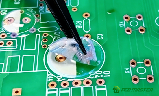
A PCB peelable solder mask is a special type of coating designed to cover parts of a PCB temporarily. Unlike permanent solder masks, it can be peeled off without leaving residue or damaging pads and traces.
Key properties include:
l Temporary protection: It shields sensitive areas such as exposed pads or small components during processes like wave soldering or selective soldering.
l Easy removal: The material is engineered to peel cleanly, preventing extra cleaning steps and reducing the risk of damaging the board.
l Compatibility with various PCB surfaces: Most peelable solder masks work with standard FR4 boards and other common substrates.
Example: During prototyping, a manufacturer might apply a peelable mask to protect fine-pitch IC pads while soldering larger connectors. After soldering, the mask can be removed in seconds, leaving the pads ready for inspection or further assembly.
Peelable solder masks come in different types depending on their application and temperature resistance. Choosing the right type ensures proper protection and easy removal.
l Standard temporary masks: These are used for general-purpose PCB protection during wave soldering or assembly. They provide reliable coverage for most single-layer or multi-layer boards.
l Selective or high-temperature variants: These masks are designed for specialized applications, such as selective soldering, reflow processes, or boards that experience higher thermal stress. They maintain peelability even after exposure to elevated temperatures.
Example: A high-temperature peelable mask might be used on a multi-layer board with lead-free soldering, ensuring the mask does not degrade during reflow while protecting sensitive components.
How Does PCB Peelable Solder Mask Differ From Regular Solder Mask?
PCB peelable solder mask differs from regular solder mask mainly in adhesion, removability, and specific use cases. While permanent masks stay bonded to the PCB for the product’s lifetime, peelable masks are temporary and can be removed cleanly after assembly, making them ideal for selective soldering, prototyping, and testing.
Adhesion and Removal
The main difference between peelable and regular solder masks lies in how they stick to the PCB.
l Lower adhesion: Peelable masks are formulated to attach lightly, allowing them to be peeled off without damaging pads, traces, or components.
l Contrast with permanent masks: Standard solder masks form a strong, permanent bond with the PCB surface. They protect the board long-term but cannot be removed without chemicals or sanding, which can damage the board.
Example: During wave soldering, a peelable mask can cover sensitive pads to prevent solder bridging. Once soldering is complete, the mask is peeled off in seconds, leaving the protected pads intact. A permanent mask, in contrast, would remain and block any further rework or inspection.
Application Process
Applying a PCB peelable solder mask is similar to a regular solder mask but with differences in curing and handling.
Steps:
l Surface preparation: Clean the PCB surface to remove oils and dust.
l Mask application: Apply the peelable solder mask by screen printing, spraying, or curtain coating depending on board design.
l Curing: Peelable masks require controlled drying or low-temperature curing to remain removable. Unlike permanent masks, they do not require high-temperature full curing.
l Inspection: Ensure uniform coverage and avoid thin spots for effective protection.
Example: A PCB manufacturer applying a peelable mask on fine-pitch IC pads ensures the mask dries evenly so that it can later be peeled without leaving residue.
Practical Use Cases
Peelable solder masks are used when temporary protection is needed during assembly, testing, or rework.
l Selective soldering: Mask pads that should not receive solder while wave-soldering other components.
l Prototyping: Protect areas during trial assemblies before final design approval.
l Testing: Shield sensitive pads during electrical tests or inspections, then remove the mask to access contacts.
Example: A company testing multi-layer PCBs may use a peelable mask to protect unpopulated pads during automated testing, ensuring no accidental solder contact or short circuits.
Comparison Table
Feature PCB Peelable Solder Mask Regular Solder Mask Adhesion Low, removable High, permanent Removal Clean peel-off Cannot remove without damage Use Case Prototyping, selective soldering, testing Long-term board protection Curing Low-temperature or partial cure Full-temperature cure Rework Easy Difficult or risky
| Feature | PCB Peelable Solder Mask | Regular Solder Mask |
| Adhesion | Low, removable | High, permanent |
| Removal | Clean peel-off | Cannot remove without damage |
| Use Case | Prototyping, selective soldering, testing | Long-term board protection |
| Curing | Low-temperature or partial cure | Full-temperature cure |
| Rework | Easy | Difficult or risky |
When Should You Use PCB Peelable Solder Mask?
PCB peelable solder masks should be used whenever temporary protection is needed during assembly, testing, or selective soldering. They are ideal for situations where pads or components must be shielded temporarily and then exposed for further work or inspection.
During Prototyping or Small-Batch Production
Peelable solder masks are especially useful during prototyping or small-batch production because they protect sensitive pads while allowing for easy rework.
l Temporary pad protection: During trial assemblies, delicate pads or fine-pitch components can be covered to prevent accidental solder bridging or contamination.
l Facilitates rework: If a prototype requires adjustments or corrections, the peelable mask can be removed without damaging the PCB.
Example: A designer testing a new PCB layout applies a peelable mask to cover unused pads. After soldering connectors, the mask is peeled away, allowing engineers to test and inspect the prototype safely.
For Selective or Complex Soldering Tasks
Peelable solder masks are ideal for selective soldering and complex PCB designs, where only certain areas should receive solder.
l Multi-layer boards: Masks can protect inner layers or specific zones while allowing wave or selective soldering on other areas.
l Fine-pitch components: Small or closely spaced components are shielded to avoid bridging or damage.
Example: On a multi-layer PCB with both through-hole and surface-mount components, peelable masks are applied to pads that should not be soldered during a wave-soldering process. This prevents defects and ensures precise soldering.
During Testing or Quality Control
Peelable masks help prevent contamination and protect critical areas during inspection or electrical testing.
l Avoid accidental damage: Sensitive pads remain shielded while automated probes or test equipment contact other areas.
l Maintain board integrity: After testing, the mask is removed cleanly, leaving the PCB ready for final assembly or shipment.
Example: A manufacturer performing electrical testing on a batch of PCBs applies peelable masks over exposed copper traces. This prevents scratches, solder residue, or short circuits, and can be removed immediately after testing.
How to Choose the Right PCB Peelable Solder Mask
Choosing the right PCB peelable solder mask requires considering both technical specifications and material quality. Selecting an appropriate mask ensures effective protection, easy removal, and compatibility with your soldering process.
Technical Considerations
When evaluating a peelable solder mask, focus on peel strength, thickness, thermal resistance, and compatibility with your soldering methods.
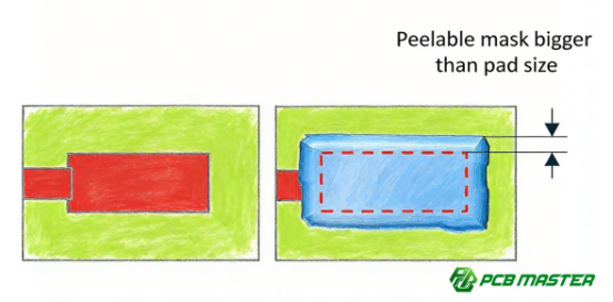
l Peel strength: The mask should adhere enough to protect pads but peel off cleanly without leaving residue. Too weak a mask may shift during soldering, while too strong a mask can damage pads.
l Thickness: Choose a mask thickness suitable for your board and component spacing. Thin masks work well for fine-pitch components, while thicker masks provide stronger protection for large pads.
l Thermal resistance: Ensure the mask can withstand the temperatures of your soldering method, such as wave soldering or lead-free reflow. High-temperature masks prevent deformation or premature peeling.
l Soldering compatibility: Confirm the mask is compatible with your process. Some masks perform better for selective soldering, while others are designed for full-board wave soldering.
Example: A manufacturer using lead-free reflow soldering selects a high-temperature peelable mask with medium peel strength. This protects fine-pitch IC pads during soldering but allows clean removal afterward.
Material Selection Tips
Beyond technical specs, material quality, supplier reliability, and proper storage are critical for consistent results.
l Reliable suppliers: Choose suppliers with proven track records and quality certifications to ensure consistent mask performance.
l Batch consistency: Variations between batches can affect adhesion, thickness, or peelability, so using the same supplier and batch improves predictability.
l Storage: Store masks according to manufacturer guidelines, usually in a cool, dry place to maintain shelf life and performance. Improper storage may reduce adhesion or peelability.
Example: A small PCB assembly shop noticed peeling issues when switching batches from a new supplier. Returning to a trusted supplier with controlled storage solved the problem, ensuring reliable mask performance.
Common Issues and Best Practices
Even with PCB peelable solder masks, manufacturers can encounter problems like poor adhesion, material incompatibility, or difficulty removing the mask cleanly. Following best practices prevents damage and ensures reliable results.
Improper Peeling or Adhesion Problems
Improper peeling or adhesion occurs when the mask sticks too strongly or not enough.
l Causes: Over-curing, dirty PCB surfaces, or using the wrong mask type for your process can cause adhesion issues. A mask that is too weak may shift during soldering, while one that is too strong can tear or lift pads.
l Prevention: Clean the PCB thoroughly before application, follow the manufacturer’s curing guidelines, and select a peelable mask with the right peel strength for your board and soldering method.
Example: A small electronics shop noticed peeling issues on fine-pitch IC pads. After properly cleaning the PCB and applying a medium-strength peelable mask, the mask removed cleanly without damaging components.
Material Incompatibility
Not all peelable solder masks work equally on every PCB substrate.
l Substrate considerations: FR-4, flexible PCBs, and metal-core boards respond differently. Some masks may not peel cleanly from flexible boards or leave residue on metal-core substrates.
l Best practices: Always check the mask manufacturer’s recommended substrates and test on a small area when using a new PCB type.
Example: A manufacturer applying a standard peelable mask to a flexible PCB saw tearing and residue. Switching to a flexible-compatible mask resolved the problem, ensuring easy removal.
Ensuring Clean Removal Without Damage
Correct peeling technique is essential to prevent pad damage or residue.
Step-by-step guidance:
1. Start at a corner or edge of the masked area.
2. Peel slowly at a low angle, keeping steady tension.
3. Avoid sharp bends or fast pulling to prevent tearing.
4. Inspect the PCB after removal and clean lightly if needed.
Example: During selective soldering, a technician initially peeled the mask too quickly, causing minor pad lifting. Adjusting to a slow, low-angle peel eliminated the problem for future assemblies.
Conclusion
Choosing the right PCB peelable solder mask and understanding its proper use can significantly improve assembly quality, simplify testing, and reduce rework. By considering factors like peel strength, thermal resistance, substrate compatibility, and proper application techniques, manufacturers can ensure reliable protection for sensitive pads and components throughout prototyping, selective soldering, and quality control processes.
For companies looking to implement these best practices efficiently, partnering with an experienced PCB and PCBA supplier can make a real difference. PCBMASTER has decades of expertise in providing high-quality PCBs and assembly services, offering guidance on material selection, mask application, and production optimization. Their deep knowledge helps costomers select the right peelable solder masks, maintain consistent quality across batches, and streamline prototyping and small-batch production.
Whether you are developing a new design or scaling up production, working with a trusted partner like PCBMASTER ensures that your boards are protected, reliable, and ready for every stage of assembly and testing.
FAQ About PCB Peelable Solder Mask
Can peelable solder mask be reused after peeling?
No, PCB peelable solder mask is generally designed for one-time use only. Once it has been applied, cured, and peeled off, the material usually loses its original shape, adhesion, and protective performance. Reusing it can lead to poor coverage, weak adhesion, or contamination on the PCB surface.
For reliable results, it is always better to apply a new peelable solder mask each time temporary protection is needed. This is especially important in selective soldering, prototyping, and testing, where clean coverage and easy removal are critical.
Is PCB peelable solder mask compatible with lead-free solder?
Yes, many PCB peelable solder masks are compatible with lead-free soldering, but you must choose a high-temperature peelable solder mask designed for that process.
Lead-free soldering usually requires higher temperatures than traditional tin-lead soldering. If the peelable mask does not have enough thermal resistance, it may soften, crack, or become difficult to remove. Always check the product specifications before use.
Tip: For wave soldering or reflow processes using lead-free solder, select a peelable solder mask rated for the required temperature range.
How long can PCB peelable solder mask stay on the PCB before removal?
A PCB peelable solder mask can usually stay on the board until the required assembly, soldering, or testing step is finished, but the exact time depends on the material type, storage conditions, and manufacturer guidelines.
Some masks are removed shortly after soldering, while others may remain in place during multiple short production steps. However, leaving the mask on for too long can make peeling harder or increase the chance of residue, especially in high heat or humid conditions.
Best practice: Remove the peelable solder mask as soon as the protected process is complete for the cleanest results.
Does PCB peelable solder mask protect against moisture or dust?
Yes, PCB peelable solder mask can provide temporary protection against dust, solder splash, and light surface contamination, and it may also help block limited short-term moisture exposure.
However, it is not a permanent environmental protection layer like a regular solder mask or conformal coating. Its main job is to protect selected PCB areas during manufacturing, not to serve as long-term moisture sealing.
If your goal is long-term protection against humidity, corrosion, or dust in the final product, you should use a permanent solder mask or an additional conformal coating instead of relying on a peelable mask.
Author Bio
Hi, I'm Carol, the Overseas Marketing Manager at PCBMASTER, where I focus on expanding international markets and researching PCB and PCBA solutions. Since 2020, I've been deeply involved in helping our company collaborate with global clients, addressing their technical and production needs in the PCB and PCBA sectors. Over these years, I've gained extensive experience and developed a deeper understanding of industry trends, challenges, and technological innovations.
Outside of work, I'm passionate about writing and enjoy sharing industry insights, market developments, and practical tips through my blog. I hope my posts can help you better understand the PCB and PCBA industries and maybe even offer some valuable takeaways. Of course, if you have any thoughts or questions, feel free to leave a comment below—I'd love to hear from you and discuss further!

