


PCB Half-Hole Technology: A Guide to Advanced Board-to-Board Connection
The demand for smaller, more efficient electronics continues to drive innovation in PCB (Printed Circuit Board) technologies. One such advancement is PCB Half-Hole Technology, a cutting-edge solution designed to enhance board-to-board connections while minimizing space and cost. This specialized technique involves the precise cutting and plating of half-holes along the edges of PCBs, creating a compact, reliable interface for electrical and mechanical connections. Widely used in high-density designs, half-holes allow for seamless, connector-free PCB interconnections, solving the challenges posed by traditional connectors. With its ability to improve both the electrical conductivity and structural integrity of connections, this technology has become a key component for manufacturers seeking to meet the demands of modern electronics.
What is PCB Half-Hole Technology?
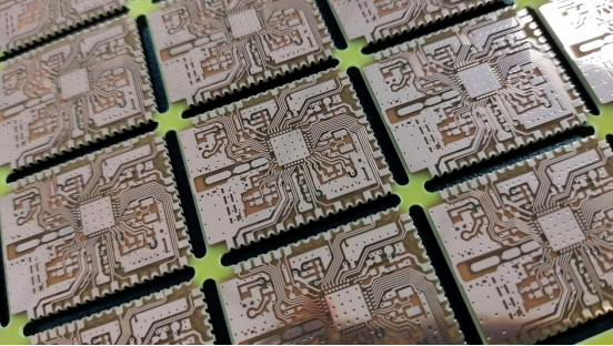
PCB Half-Hole, also known as Castellated Hole, Plated Half-Holes, or Edge Plated Holes, is a specialized structure created on the edges of PCBs. The process involves drilling, electroplating, and then precisely cutting the hole along its centerline to form a semi-circular, metalized hole. This technology enables high-density, miniaturized, and cost-effective board-to-board electrical connections and mechanical fixing. It is widely used in advanced PCB manufacturing, especially for module-to-mainboard connections. PCBMASTER has refined this core process over many years, providing highly adaptable custom solutions for various industries.
Design and Metallization of Half-Holes
PCB half-holes are created by drilling and shaping processes that preserve 50%-70% of the hole wall. The remaining material is removed, creating a metalized, conductive interface. The hole walls undergo metallization treatment, with copper plating thickness typically controlled between 20-30μm. This dual-purpose structure serves both electrical conduction and mechanical positioning, making it ideal for direct board-to-board connections. Two PCBs can be interconnected by nesting their half-holes without the need for extra connectors.
Difference Between Half-Holes and Through-Holes
The main differences between half-holes and traditional through-holes lie in both structure and function. A through-hole is a fully-through structure used for inter-layer electrical conduction but does not require precision for external connections. On the other hand, a half-hole is a semi-through structure primarily used for board-to-board connections. This structure demands stricter control over hole wall flatness and dimensional tolerances to ensure the boards can connect tightly. Without precision, the boards may not align properly, leading to potential connection failure.
Precision Control in Half-Hole Manufacturing
PCBMASTER has established strict production standards for half-hole manufacturing. The company’s engineering team is skilled in accurately controlling the entire production process to avoid dimensional discrepancies. This ensures both electrical conductivity and structural stability meet the highest standards. Through its expertise, PCBMASTER ensures that half-holes are produced with the utmost precision, avoiding issues like poor conductivity or misalignment during the final assembly.
PCBMASTER Half-Hole Process: Design and Processing Key Points
Minimum Half-Hole Size Requirements
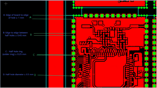
PCBMASTER recommends a minimum finished hole diameter of 0.5mm (with a maximum limit of 0.4mm) for its half-hole process. The key requirement for creating half-holes of this size is that the center of the hole must align with the edge of the PCB, meaning that 0.25mm (maximum 0.4mm) of the hole body must remain inside the board. This is a critical design guideline validated through extensive production experience. Failing to meet this requirement can result in copper layer detachment from the hole wall or copper-free holes, leading to reduced yield rates in the final half-hole PCB product.
Half-Hole Spacing Design Guidelines
PCBMASTER’s half-hole process standard specifies that the minimum finished hole diameter is 0.5mm, and during manufacturing, process compensation is applied to the hole size. After compensation, the distance between half-holes must be at least 0.35mm, so the design phase should ensure that the spacing between half-holes is ≥0.45mm. The width of the corresponding pads after compensation should be at least 0.25mm. Additionally, a solder mask bridge must be placed between pads that correspond to the half-hole openings. PCBMASTER's engineering team strongly recommends that clients adhere to these design standards to avoid issues like plating failures or solder bridging during the manufacturing process.
Standardized Production Process for Half-Hole PCBs
The design logic behind half-holes is that the metallized hole is split, with half of the hole inside the PCB and the other half exposed on the outside. The key requirement for this product is to ensure the copper layer on the hole wall is intact, preserving the integrity of the hole for component insertion. PCBMASTER has developed a standardized, highly stable production process consisting of the following steps:
1. Drilling: Drilling is performed along the edge of the PCB according to the design specifications. This step requires precise control of both the depth and position of the holes to ensure the size and location of the half-holes meet design requirements.
2. Copper Deposition: A thin layer of copper is deposited onto the drilled hole walls to improve conductivity and adhesion.
3. Board Surface Electroplating: The entire PCB surface is electroplated to enhance its conductivity and corrosion resistance.
4. Outer Layer Circuit Fabrication: The required circuit patterns are created on the outer copper layer.
5. Pattern Electroplating: The circuit patterns are electroplated locally to enhance their conductivity and wear resistance.
6. Lead-Tin Plating (optional): If needed, a layer of lead-tin alloy is applied to the PCB surface to improve its solderability and corrosion resistance.
7. Milling Half-Hole: Using a milling cutter, the hole on the PCB edge is milled to leave a half-hole structure. This step requires precise control over the milling depth and trajectory to ensure the half-hole meets the design specifications.
8. Stripping: The protective resist layer and any other unnecessary coatings on the PCB surface are removed.
9. Etching: A chemical etchant is used to remove the unprotected copper foil, forming the required circuit patterns.
10. De-soldering (if lead-tin plating was applied): If lead-tin alloy was applied, it is removed during this step to eliminate any excess solder.
Design Considerations to Prevent Solder Bridging During Assembly
When the pins for half-holes are designed as rectangular, some engineers may increase the pad width to match the hole diameter, aiming to ensure the correct ring size. However, this can lead to an issue where the pad spacing is overlooked, resulting in solder bridging during assembly. To address this common design mistake, the PCBMASTER engineering team offers the following professional design advice: only the corresponding hole ring needs to be created for the half-hole. There is no need to enlarge the entire pin width, as the outer part of the half-hole will be removed during the milling process. Excessively widening the pins does not provide any practical benefit and can cause unnecessary complications in the process.
Special Processing Requirements for Half-Slot Holes
If the half-hole is a slot-type structure, PCBMASTER requires an additional guide hole with a diameter of ∮0.8-1.1mm at both ends of the slot. These guide holes must be placed in a separate drilling layer. Additionally, a second drilling process is needed before milling the half-hole. This is done to prevent the copper layer from lifting due to uneven stress during the milling of the slot hole. This processing requirement is part of PCBMASTER's optimization for slot-type half-holes, which can significantly improve the yield of this type of hole.
Guidelines for Making Half-Hole Tooling for Improved Precision and Efficiency
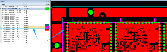
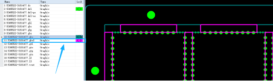
To enhance the precision and manufacturing efficiency of half-holes, PCBMASTER has established specific guidelines for creating half-hole tooling: The PCB panel must include a 1.6mm wide closed outer frame, referred to as GKO2 (used specifically for milling half-holes before etching). If the product is a SET panel, the GKO2 frame must be made within the SET, and the closed area must not extend into the inner part of the board. The primary purpose of this design is to facilitate the process of outlining the half-hole area, allowing for quick and accurate identification of the half-hole processing region. This is an essential step in PCBMASTER's efforts to improve production efficiency and maintain tight control over the manufacturing process.
PCB Half-Hole Panelizing and Connection Design
When panelizing half-hole PCBs, it is essential to leave adequate spacing between the half-holes to facilitate the milling process. However, this requirement is often overlooked during the design phase. This is because layout engineers rarely visit PCB factories to understand how half-holes are produced. As a result, for products with special half-hole designs, some engineers may panelize them as if they were standard boards, without leaving sufficient space between the holes and using V-CUT for separation. This can cause the copper around the half-holes to be damaged or removed by the V-CUT blade, resulting in holes with no copper, rendering the product unusable.
For half-hole PCBs delivered as individual boards, if half-holes are located around the entire edge of the PCB, the lack of process boundaries and MARK points can prevent the factory from proceeding with PCB assembly. Therefore, panelizing the product for delivery is the optimal choice for such cases. Regarding the panelization design of half-hole PCBs, PCBMASTER’s engineering team offers the following professional advice: avoid using V-CUT for panelizing when half-holes are on one side, especially if half-holes are located on all four edges. Typically, connection bridges are added at the four corners or areas without half-holes. These connection bridges can be created using stamp holes, with each bridge width being greater than 2mm to prevent PCB breakage or deformation during manufacturing and assembly.
Half-Hole PCB Routing Process
As half-hole PCBs are panelized with connection bridges, PCBMASTER recommends using high-precision, low-stress CNC routing machines for the panel separation after PCB assembly. This ensures that the edges of the separated panels are free of burrs, sharp edges, and remain smooth and even. This guarantees that the boards meet the requirements for subsequent assembly and usage. PCBMASTER’s in-house production facility is equipped with professional, high-precision routing equipment, offering integrated half-hole PCB production and routing services for our customers.
Half-Hole and Drilling Circuit Production Requirements
PCBMASTER has established specific standards for the drilling and circuit production of half-hole boards: the drilling process follows the same procedures as for standard PCBs, with diameter compensation applied according to standard processes. The minimum finished half-hole diameter is typically designed to be 0.5mm. The board’s outer shape is processed with copper trimming, and then the standard process is followed for stacking and fabricating the circuit pads. The spacing between the pads must be ≥0.25mm. The PCBMASTER production team strictly adheres to these standards throughout the entire process, from design to production, to completely avoid the risk of solder bridging during the final soldering phase.
Half-Hole Solder Mask Production Requirements
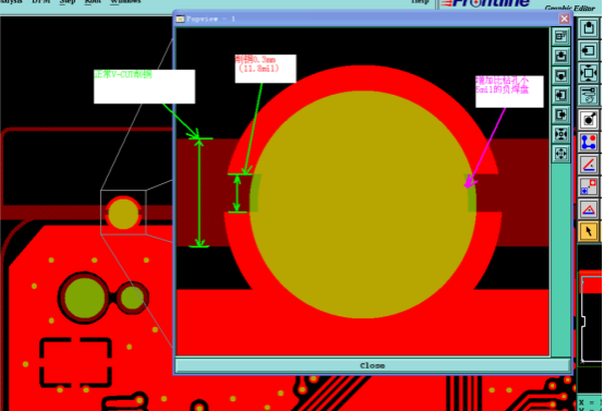
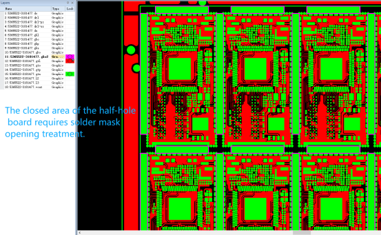
During the solder mask production phase for half-hole PCBs, PCBMASTER enforces strict process guidelines: the closed area of the half-hole board must have a solder mask window treatment. If this area is not windowed, ink may seep into the half-hole walls, negatively affecting the hole's conductivity and solderability. Additionally, no windows should be created between the circuit pads corresponding to the half-hole. If the process cannot guarantee the creation of a solder mask bridge, the PCBMASTER engineering team should be contacted in advance. Based on the specific situation, the team will recommend increasing the half-hole spacing as a solution. If the pad spacing is insufficient, solder bridging may occur during the soldering stage, leading to potential faults.
Conclusion
PCBMASTER has been focused on high-precision PCB manufacturing for many years, and has established a comprehensive process control and quality management system specifically for the half-hole process. From initial design coordination and process optimization, to standardized production and full-process inspection, and finally to panel separation and delivery, PCBMASTER offers a one-stop service for half-hole PCBs and PCB assembly. With mature process technology and stringent quality control, we are able to meet the high-precision and high-stability production demands of clients across various industries for half-hole PCBs.
FAQs
1. What are the primary applications of PCB Half-Hole Technology?
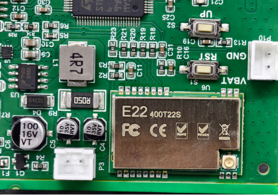
PCB Half-Hole Technology is primarily used in high-density, miniaturized electronic designs, particularly for module-to-mainboard connections. It is ideal for applications where space is limited and traditional connectors are too large or costly. Common uses include wearable devices, mobile phones, IoT products, and other compact electronic systems that require reliable board-to-board connections.
2. How does PCB Half-Hole Technology improve PCB assembly?
By eliminating the need for external connectors, PCB Half-Hole Technology allows for more streamlined and compact designs. It provides a direct electrical and mechanical connection between PCBs, reducing assembly time and potential points of failure. This approach improves both the reliability and performance of the final product by minimizing the number of components that need to be assembled.
3. What challenges are associated with designing PCBs using Half-Hole Technology?
Designing PCBs with Half-Hole Technology requires precise control over hole size, spacing, and metallization to ensure proper electrical conductivity and mechanical stability. Engineers must also account for the accuracy of hole alignment between stacked boards, as any misalignment could lead to connection failures. The small size of the holes also presents challenges in terms of achieving consistent quality during manufacturing.
4. Can Half-Hole PCBs be used in high-frequency or high-power applications?
Yes, Half-Hole PCBs can be used in high-frequency or high-power applications, but there are additional considerations. The precise metallization of the half-holes ensures reliable electrical connections, but the design must take into account factors like impedance control and heat dissipation, especially for high-frequency signals or high-power components. Proper manufacturing techniques and material choices are crucial for maintaining performance under these conditions.
5. What are the advantages of using PCBMASTER's Half-Hole Technology over traditional methods?
PCBMASTER’s Half-Hole Technology offers several advantages, including reduced space requirements, cost savings from eliminating external connectors, and improved connection reliability. With years of experience, PCBMASTER ensures precise manufacturing through a standardized process that minimizes defects, improves yield rates, and delivers high-quality, stable PCBs. Additionally, the technology allows for easy customization, making it suitable for a wide range of industries and applications.
Author Bio
Hi, I'm Carol, the Overseas Marketing Manager at PCBMASTER, where I focus on expanding international markets and researching PCB and PCBA solutions. Since 2020, I've been deeply involved in helping our company collaborate with global clients, addressing their technical and production needs in the PCB and PCBA sectors. Over these years, I've gained extensive experience and developed a deeper understanding of industry trends, challenges, and technological innovations.
Outside of work, I'm passionate about writing and enjoy sharing industry insights, market developments, and practical tips through my blog. I hope my posts can help you better understand the PCB and PCBA industries and maybe even offer some valuable takeaways. Of course, if you have any thoughts or questions, feel free to leave a comment below—I'd love to hear from you and discuss further!


