


Solder Mask Opening and Bridge Design DFM Guide for Reliable PCB Manufacturing
Solder mask openings and bridge design are critical for PCB reliability, especially in high-density and complex layouts. With years of experience in manufacturing PCBs and PCBAs, PCBMASTER understands the challenges designers face in preventing short circuits, solder bridges, and other defects. This guide shares practical insights and proven strategies to help designers optimize solder mask spacing, ensure manufacturability, and deliver boards that perform flawlessly from prototype to mass production.
What is Solder Mask Opening and Bridge Design DFM, and Why Is It Important?
Solder Mask Opening and Bridge Design DFM ensures proper spacing and coverage of solder mask openings and bridges on a PCB, preventing solder shorts, improving reliability, and enabling manufacturable, high-quality boards.
What is a solder mask opening, and what is its function?
A solder mask opening is a window in the solder mask layer that exposes the copper beneath for soldering or testing.
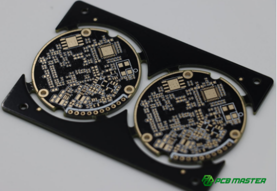
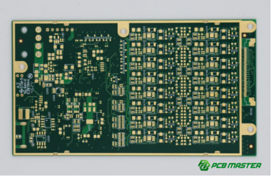
A solder mask opening, also called a “solder mask window,” is a carefully designed area where the protective solder mask is removed, exposing the copper pad, via, or trace. Its main function is to allow solder to bond to the PCB surface during assembly while protecting surrounding areas from accidental solder bridging. For example, in a small BGA (Ball Grid Array) component, each solder ball must have its own clear opening to ensure correct soldering. Without proper openings, solder may spread to nearby pads, causing short circuits.
What is the role of solder mask bridges, and what reliability risks do they prevent?
Solder mask bridges act as protective barriers between openings, preventing short circuits and improving reliability.
Solder mask bridges are the narrow areas of solder mask that remain between two openings. They prevent molten solder from flowing across adjacent pads and creating electrical shorts. For high-density designs, such as 0.5mm pitch BGA or QFN packages, solder mask bridges are essential to maintain proper insulation between tiny pads. Without adequate bridges, tiny solder connections may short during reflow soldering, leading to board failures.
Real-life case: a smartphone PCB failed QA due to solder bridging between dense IC pads, which could have been avoided with wider solder mask bridges.
What soldering problems and electrical shorts can result from poor design?
Poor solder mask opening and bridge design can cause solder bridges, solder balls, and defective connections, leading to short circuits and board failure.
If solder mask openings are too close or bridges are too thin, solder can flow into unintended areas during reflow or wave soldering. Common issues include:
Solder bridging – short circuits between adjacent pads.
Solder balls or debris – tiny balls of solder that may fall onto other traces, causing intermittent or permanent shorts.
Inspection and cosmetic failures – even if no short occurs, poor appearance may be flagged by AOI (Automated Optical Inspection).
Example: On a high-density PCB with 0.4mm pitch connectors, inadequate solder mask spacing led to repeated failures in mass production.
How does PCBMASTER provide high-quality DFM verification?
PCBMASTER offers professional DFM checks, combining software validation and manufacturing experience to ensure solder mask openings and bridges meet reliability standards.
PCBMASTER uses advanced DFM (Design for Manufacturability) tools and years of hands-on PCB and PCBA experience to check:
l Solder mask to solder mask clearances
l Bridge widths for high-density components
l Compliance with fabrication limits for mass production
Steps include automated software checks, manual review by engineers, and confirmation with the board factory. This process ensures that solder mask openings are neither too small (causing coverage issues) nor too close (causing shorts).
Example: For a 0.5mm pitch BGA, PCBMASTER verified solder mask bridge widths and ensured over 95% first-pass yield in production.
How Should the Minimum Spacing Between Solder Mask Openings Be Designed?
The minimum spacing between solder mask openings should be designed based on PCB density and manufacturing capability, typically ≥0.2 mm for standard boards, 0.13 mm for high-density designs, and never below 0.075 mm to ensure reliability and prevent solder bridging.
What are the common spacing standards and recommended values?
The minimum spacing between solder mask openings depends on PCB density and manufacturing capability, with standard, high-density, and absolute minimum guidelines.
Designing proper spacing between solder mask openings is critical to prevent solder bridging and ensure manufacturability. Typical spacing rules are:
l Standard Applications: A safe minimum is ≥ 0.2mm (8mil). Most PCB factories can easily handle this spacing, making it suitable for general electronics.
l High-Density Designs: For mobile devices, HDI boards, or dense connectors, spacing can be reduced to 0.13mm (5mil) with precision fabrication equipment.
l Absolute Minimum: Anything below 0.075mm (3mil) is extremely risky and usually not recommended, as it may lead to production failures.
Comparison Table: Minimum Solder Mask Spacing Guidelines
| Application Type | Minimum Spacing | Notes |
| Standard PCB | 0.2mm (8mil) | Safe, easy for most manufacturers |
| High-Density PCB | 0.13mm (5mil) | Requires advanced equipment, higher cost |
| Absolute Minimum Limit | 0.075mm (3mil) | Not recommended; high risk of solder bridging and low yield |
What risks occur if spacing is insufficient?
Too little spacing between solder mask openings can cause solder bridging, solder balls, and cosmetic or inspection failures, reducing PCB reliability.
Solder mask bridge breakage or absence causing shorts
When the solder mask bridge between openings is too thin or missing, molten solder can flow across adjacent pads, creating short circuits. This is especially dangerous for small-pitch components like BGA or QFN.
Real-life example: a dense connector PCB failed during assembly because the bridges were narrower than 0.1mm, causing multiple shorts.
Solder balls or debris formation and potential hazards
Narrow spacing can trap excess solder, forming tiny balls or debris. These can move across the board and cause intermittent or permanent shorts.
Case study: In a consumer electronics PCB, misplaced solder balls led to intermittent device failure, requiring rework.
Cosmetic defects and inspection difficulties
Even if no short occurs, very thin solder mask bridges or irregular openings can be flagged by AOI machines or appear visually defective. This can delay production approval and reduce perceived product quality.
How to check solder mask spacing in PCB design tools
PCB design software includes DFM and clearance tools to automatically verify solder mask-to-solder mask spacing.
Most PCB CAD tools (Altium, KiCad, OrCAD) have Design Rule Check (DRC) or DFM verification features. Steps include:
1. Set the minimum solder mask-to-solder mask clearance according to your design rule (e.g., 0.2mm for standard boards).
2. Run the DRC to highlight any violations.
3. Adjust pad size, solder mask expansion, or reposition pads as needed.
4. Export the Gerber files with clear solder mask layers for manufacturer review.
Practical tip: Always confirm with the PCB supplier, as some factories may have tighter or looser process capabilities, especially for high-density HDI boards.
What Should Be Considered for Solder Mask Opening Design in Different Component Types?
Solder mask opening design for different components should account for pad size, solder mask bridge width, component pitch, thermal or high-current areas, board edges, and gold finger or shield pads to prevent shorts and ensure reliable soldering.
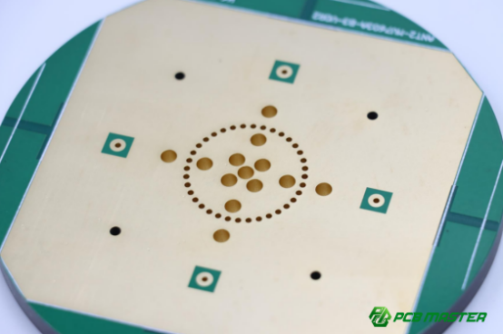
BGA / QFN Fine-Pitch Components
BGA and QFN components require careful solder mask bridge design and pad sizing to prevent shorts and ensure reliable soldering.
Recommended solder mask bridge width and pad diameter ratio
For fine-pitch components like BGA (0.5mm pitch) or QFN, the solder mask bridge between pads must be wide enough to prevent solder shorts. A common guideline is for the bridge width to be approximately 0.2–0.25mm, with pad diameters 0.25–0.3mm.
Example: On a 0.4mm pitch BGA, if the bridge is too narrow, solder can flow between pads during reflow, causing failures.
Application of Solder Mask Defined Pads (SMD Pads)
Solder Mask Defined Pads (SMD Pads) are used when solder mask openings are smaller than the copper pads. This increases the effective solder mask bridge width, helping prevent shorts. For high-density boards, SMD pads also help control solder volume and improve wetting.
Case: A smartphone HDI PCB with 0.4mm BGA pitch achieved a 95% first-pass yield by using SMD pad design.
High-Current Traces and Thermal Pads
Large copper areas for current or heat require special solder mask spacing to prevent bridging with nearby pads.
Clearance considerations for large openings near small pads
When designing large solder mask openings for thermal pads or high-current traces, maintain adequate spacing from adjacent small pads to prevent molten solder from flowing.
Example: A power supply PCB with 10A traces included 0.3mm clearance from nearby signal pads, avoiding shorts during wave soldering.
Solder Mask Openings Near Board Edges, V-Cuts, and Routing Lines
Openings near board edges or V-Cut lines must account for mechanical stress during separation.
Impact of panelization and routing on solder mask openings
Openings too close to edges or V-Cuts may be damaged during board separation, exposing copper and risking shorts.
Rule: maintain ≥0.5mm distance from board edges or V-Cut lines.
Case study: A PCB with 0.2mm edge clearance had torn solder mask after depanelization, causing electrical failures.
Shielding Pads and Gold Finger Areas
Large openings for shielding or gold fingers require careful spacing to avoid shorts and ensure reliable contact.
Clearance for large solder mask openings near other pads
Shielding pads often use long solder mask openings. Ensure sufficient distance (≥0.5mm) from nearby signal pads to prevent solder overflow.
Example: In a communication module, maintaining proper spacing avoided solder bridges during shield assembly.
Gold finger opening size and beveled edge requirements
Gold finger pads must have openings slightly larger than the copper pads and include beveled edges for easy insertion and reliable contact. This prevents solder mask from covering the contact area.
Rule: open each side ~0.2mm larger than the pad.
How to Ensure Solder Mask Opening Design Meets Manufacturing Feasibility?
To ensure solder mask opening design is manufacturable, provide accurate Gerber files, account for surface finish effects on pad dimensions, and maintain adequate clearance from board edges and panelization lines.
How to provide accurate Gerber files?
Accurate Gerber files ensure that the PCB manufacturer interprets solder mask openings and bridges correctly, avoiding production errors.
Key points for GTS / GBS files
GTS (Top Solder Mask) and GBS (Bottom Solder Mask) files define where the solder mask is removed. Ensure that these files accurately match your design intent, with clear, precise openings and no extra copper exposure.
Real-world example: A misaligned GTS file caused unintended pad exposure on a dense HDI PCB, leading to solder bridging in assembly.
Best practice: always double-check Gerber layers and perform a DFM review with the board manufacturer.
Checking negative-output solder mask layers
If using negative solder mask output, where the exposed areas are inverted, it is critical to verify that the negative polarity does not accidentally block pads or expose unwanted copper.
Steps: inspect in Gerber viewer, confirm with manufacturer, and adjust openings if needed.
Example: Negative-output misinterpretation caused solder mask over a QFN pad, preventing proper soldering.
How does surface finish affect solder mask openings?
Different surface finishes can slightly change pad dimensions, affecting solder mask bridge width and spacing, especially in high-density designs.
Common surface finishes and micron-level variations
Common finishes include HASL (lead-free), ENIG, ENEPIG, and immersion silver. Each can slightly increase or decrease pad dimensions by a few microns, which may impact solder mask coverage.
Example: ENIG pads may appear slightly smaller than copper pads, so solder mask openings must account for this to prevent pad exposure issues.
Compensating for bridge width in high-density designs
For dense BGA or fine-pitch ICs, account for potential pad shrinkage or growth due to surface finish by slightly increasing solder mask bridge width.
Case study: A 0.4mm pitch BGA used an additional 0.01–0.02mm bridge width to maintain insulation after ENIG plating.
How should panelization and board-edge openings be handled?
Openings near panel edges or V-Cut lines must maintain adequate clearance to prevent damage during depanelization.
Minimum distance from depanelization lines ≥0.5mm
Solder mask openings too close to board edges or V-Cuts can tear during separation, exposing copper and risking shorts.
Rule of thumb: maintain ≥0.5mm clearance from any edge, V-Cut, or scoring line.
Example: A PCB panel with 0.3mm clearance had torn solder mask at the edges after routing, causing electrical failures in production.
What Rules Should Be Followed for Solder Mask Opening Size and Shape Design?
Solder mask openings should be slightly larger than copper pads, avoid sharp angles or spikes, and cover isolated copper fragments to ensure proper soldering, prevent mask peeling, and reduce short-circuit risks.
What are the rules for solder mask opening expansion?
Solder mask openings should be slightly larger than copper pads to ensure proper coverage and alignment during manufacturing.
Single-side expansion 0.05mm ~ 0.075mm
A common guideline is to expand each side of the solder mask opening 0.05–0.075mm (2–3 mils) beyond the copper pad size. This compensates for minor misalignments during printing and ensures pads remain exposed for soldering.
Example: A QFN pad with 0.3mm diameter had a 0.07mm solder mask expansion on each side, preventing accidental coverage during assembly.
LDI high-precision designs can reach 1 mil
For Laser Direct Imaging (LDI) technology, which provides higher precision, solder mask expansion can be as small as 1 mil (~0.025mm). This allows tighter spacing for high-density designs without risking shorts.
Example: A 0.4mm pitch BGA used 1 mil expansion, achieving high manufacturability without reducing pad accessibility.
How should sharp angles, spikes, and isolated copper be handled?
Avoid sharp corners, long spikes, or small isolated copper pieces in solder mask openings to prevent stress-related ink failure and short circuits.
Prevent exposure stress concentration and mask peeling
Sharp angles or pointed spikes in solder mask openings create stress points during UV exposure and development, which may cause the solder mask to peel or crack.
Example: A PCB with triangular solder mask tips on a large pad experienced ink delamination during reflow, leading to exposed copper shorts. Rule: round corners or avoid extreme spikes.
Cover large isolated copper fragments to reduce short risk
Small isolated copper pieces or fragments on large copper areas should be covered by solder mask to prevent unintentional solder bridging or shorts.
Example: On a power PCB with isolated copper islands, leaving them exposed led to minor shorts; applying solder mask coverage solved the issue.
How Does PCBMASTER’s DFM Verification Process Improve Design Reliability?
PCBMASTER’s DFM verification process improves design reliability by checking solder mask spacing with software, confirming bridge widths for high-density components, coordinating with manufacturers, and reducing defects to enhance mass production yield.
How are solder mask clearances checked using software or third-party tools?
PCBMASTER uses CAD software and third-party DFM tools to automatically verify solder mask-to-solder mask spacing, catching potential issues before manufacturing.
By running automated Design Rule Checks (DRC) and DFM verification, software can highlight violations such as insufficient solder mask bridges or openings that are too close.
Example: For a high-density HDI board, DFM software flagged several 0.12mm gaps below the recommended 0.13mm, allowing engineers to adjust pad placement before production.
How is solder mask bridge confirmation handled for special components and high-density boards?
PCBMASTER specifically reviews BGA, QFN, and other fine-pitch or high-density components to ensure solder mask bridges are wide enough for manufacturability and reliability.
Special attention is given to components with small pitches or dense layouts. Engineers inspect solder mask bridges around each pad, confirming they meet minimum width requirements and avoid shorts.
Example: A 0.4mm pitch BGA required using Solder Mask Defined Pads to maintain 0.1mm bridge width, ensuring successful assembly.
How does communication with the PCB manufacturer improve design feasibility?
Sharing design files and receiving written feasibility confirmation ensures the PCB manufacturer can produce the design reliably without misinterpretation.
PCBMASTER sends Gerber and DFM reports to manufacturers and confirms that solder mask openings, bridges, and edge clearances meet their process capabilities. This reduces production risk.
Example: Coordination with a PCB vendor allowed slight adjustment of large thermal pad openings, preventing solder overflow during wave soldering.
How does PCBMASTER’s DFM process improve mass production yield?
Thorough DFM checks and manufacturer collaboration minimize defects, leading to higher first-pass yields and more reliable boards.
By systematically reviewing solder mask design, pad spacing, and component placement, PCBMASTER reduces solder bridging, peeling, and shorts.
Case overview: After implementing DFM verification, a mobile HDI PCB project reported significantly fewer assembly failures, smoother production, and improved product reliability, demonstrating the value of structured DFM processes.
What Are Common Solder Mask Opening Design Problems and Their Solutions?
Common solder mask opening design problems—such as pad short circuits, solder balls, insufficient BGA bridges, and large thermal pad solder overflow—can be solved by proper spacing, bridge width adjustments, precise mask alignment, and protective measures for high-current or large-area pads.
How to prevent pad short circuits?
Pad short circuits can be prevented by maintaining sufficient solder mask bridge width and proper spacing between openings.
Short circuits often occur when solder mask bridges are too narrow or openings are too close. Solution: follow minimum spacing guidelines (≥0.2mm for standard boards, 0.13mm for high-density boards) and use Solder Mask Defined Pads for fine-pitch ICs.
Example: A 0.5mm pitch BGA had 0.18mm bridges, which were widened to 0.22mm in the design stage, eliminating solder shorts during reflow.
How to reduce solder balls and soldering defects?
Solder balls and defects are minimized by correct pad size, proper solder mask alignment, and controlling solder volume.
Excessive solder or misaligned mask openings can create tiny solder balls or uneven joints. Steps to reduce defects include precise pad sizing, checking solder mask alignment, and optimizing paste printing and reflow profiles.
Example: On a high-density connector, adjusting solder paste stencil thickness and confirming mask coverage reduced solder balls by over 80%.
How to optimize insufficient solder mask bridges on high-density BGA?
Insufficient bridges can be addressed by adjusting solder mask openings, using SMD pads, and verifying clearances with DFM tools.
Fine-pitch BGAs often have bridges narrower than manufacturing tolerances, causing shorts. Solutions include slightly reducing pad sizes, increasing mask bridge width, and confirming with DFM software.
Example: A 0.4mm pitch BGA board used 1 mil expansion and SMD pads, preventing shorts while maintaining solderability.
What protective measures are needed for large thermal pad openings?
Large thermal or high-current pad openings require sufficient clearance from surrounding pads and may include partial solder mask coverage to control solder flow.
Without proper precautions, molten solder can spread and create bridging. Solutions include maintaining ≥0.3mm clearance from nearby pads, splitting large thermal pads into smaller segments, or adding a thin mask dam.
Example: A power module PCB split a 50mm² thermal pad into four segments with solder mask dams, preventing overflow during wave soldering.
Conclusion
Mastering solder mask opening and bridge design is key to creating reliable, high-quality PCBs. By following proper spacing rules, optimizing bridge widths, verifying designs with DFM tools, and collaborating with experienced manufacturers like PCBMASTER, designers can prevent shorts, solder defects, and assembly issues. Applying these best practices not only improves yield and product reliability but also ensures smooth mass production, making every board a success.
FAQs
Why can’t the minimum spacing between solder mask openings be less than 0.075mm?
A minimum spacing below 0.075mm risks solder mask bridges failing during manufacturing, which can cause adjacent pads to connect and create shorts, especially on fine-pitch components. Maintaining ≥0.075mm ensures manufacturability and reduces defect rates.
How should BGA solder mask bridges be designed to minimize short-circuit risk?
For BGAs, ensure solder mask bridges are wide enough relative to pad size and pitch, typically maintaining ≥0.2mm for 0.5mm pitch BGAs. Using Solder Mask Defined Pads (SMD) can further control solder flow and prevent bridging between fine-pitch balls.
What DFM considerations are important for gold finger solder mask openings?
Gold finger openings should be slightly larger than the contact pad, include beveled edges to prevent solder coverage, and maintain ≥0.5mm clearance from nearby traces to ensure reliable electrical contact and reduce wear during insertion.
How is the solder mask opening expansion determined?
Solder mask openings are generally expanded 0.05–0.075mm on each side of the copper pad to compensate for printing alignment and exposure tolerances; high-precision LDI processes can reduce expansion to 1 mil (~0.025mm) for fine-pitch designs.
How do large solder mask openings affect wave or reflow soldering?
Large openings can cause solder to spread excessively, creating shorts or uneven joints. Solutions include maintaining sufficient clearance from neighboring pads, splitting the opening, or adding partial mask “dams” to control solder flow and ensure proper wetting.

