


IC Substrate Fine Circuit Manufacturing: Techniques, Semi-Additive Process, and Ultra-Fine Lines
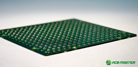
Fine circuits on IC substrates refer to the tiny copper pathways on a package board that connect different parts of an integrated circuit (IC). These circuits are responsible for transmitting signals and power between chips, ensuring the IC operates reliably. Over the years, the line widths and spacing of these circuits have evolved from the original 50μm/50μm to as small as 10μm/10μm, enabling electronic devices to become more powerful and compact.
This advancement is made possible by what is known as “ultra-connection technology,” which allows numerous fine lines and vias to interconnect without causing short circuits or signal loss. For instance, modern smartphones and high-performance processors rely on these ultra-fine connections to integrate more functionality into smaller spaces.
The current industry trend is moving toward finer wiring, thinner copper layers, and higher-density layouts. Along with these technological advancements come new challenges, such as maintaining high yield rates, preventing circuit delamination, and ensuring signal integrity.
So, how can companies upgrade their technology while still ensuring production efficiency and product reliability? As a professional supplier with years of extensive experience in IC substrate and PCB/PCBA manufacturing, PCBMASTER provides a comprehensive overview of key fine-line technologies and advanced processes, including semi-additive process optimization, ultra-thin copper layer fabrication, and high-precision circuit design. Our goal is to help engineers gain a deep understanding of these cutting-edge technologies and apply them effectively, achieving high-reliability IC substrate production while minimizing production risks and costs.
What Are the Main Manufacturing Methods for IC Substrate Fine Circuits?
The main methods for producing fine circuits on IC substrates include subtractive, additive, and semi-additive processes. Each approach has unique steps, advantages, and limitations, depending on the desired line width, spacing, and board type. PCBMASTER uses these processes to achieve high-precision IC substrates for modern electronics, balancing yield, reliability, and manufacturing efficiency.
What Is the Subtractive (Removal) Process and How Does It Work?
The subtractive process removes copper from a fully laminated board to form the desired circuit pattern. First, a photosensitive layer or screen-printed resist is applied to the copper surface. This layer is patterned using photolithography or screen printing, exposing the areas where copper should remain. The unprotected copper is then chemically etched away, leaving only the circuit lines.
This method is widely used in HDI and Bμm boards, especially for line widths around 50μm. Its main advantages are simplicity and cost-effectiveness. However, it faces limitations when trying to achieve finer circuits below 50μm/50μm, because over-etching or uneven copper thickness can reduce yield. For example, producing 40μm lines with traditional subtractive etching often leads to broken circuits or reduced reliability.
What Is the Additive Process and When Is It Used?
The additive process builds up copper only where the circuit is required. Conductive metal is selectively deposited onto the substrate surface, forming the circuit pattern directly. This avoids removing large amounts of copper, which can reduce waste and improve precision.
The additive method is suitable for ultra-fine circuits, but it has some challenges. Deposited copper may have bonding or surface roughness issues, and the process can be slower and more expensive than subtractive etching. PCBMASTER uses additive techniques selectively, especially when working on high-density boards with line widths below 50μm, where precise deposition provides better control over fine features.
What Is the Semi-Additive Process (SAP) and Why Is It Preferred for Ultra-Fine Lines?
The semi-additive process (SAP) combines the advantages of subtractive and additive methods. Initially, a very thin copper layer is coated on the substrate. Circuit patterns are then defined using photolithography, followed by copper electroplating to thicken the lines only where needed. Finally, a differential etching step removes the remaining thin copper from non-circuit areas.
SAP allows for finer line widths and closer spacing, often reaching 15μm/15μm or smaller, which is difficult with purely subtractive or additive methods. Improved SAP techniques also reduce side-etching and enhance circuit reliability. PCBMASTER applies SAP for high-density IC substrates, using controlled electroplating and etching to achieve ultra-fine, highly reliable circuits for smartphones, high-performance processors, and advanced electronics.
Comparison Table of Main Manufacturing Methods for IC Substrate Fine Circuits
The table below provides a side-by-side comparison of the main manufacturing methods for IC substrate fine circuits, highlighting their processes, typical line widths, advantages, limitations, and practical applications.
| Process | How It Works | Typical Line Width / Spacing | Advantages | Limitations / Challenges | PCBMASTER Application |
| Subtractive (Removal) | Copper is fully laminated; resist is applied and patterned; unprotected copper is etched away | ~50μm/50μm | Simple, cost-effective, widely used in HDI/Bμm boards | Hard to achieve <50μm lines; over-etching can reduce yield | Used for standard HDI and Bμm boards where moderate precision is acceptable |
| Additive | Copper is selectively deposited only where circuit lines are needed | Can reach <50μm | Less copper waste, better precision for fine features | Slower, more expensive, potential bonding or surface issues | Applied for high-density boards where precise deposition improves line quality |
| Semi-Additive Process (SAP) | Thin copper layer applied; pattern defined by photolithography; copper electroplated; remaining thin copper etched away | 15–25μm / 15–25μm (sometimes smaller) | Combines subtractive and additive advantages; enables ultra-fine lines; high reliability | Requires precise plating and etching control | Preferred for ultra-fine IC substrate circuits, smartphones, high-performance processors |
Why Is the Conventional Subtractive Method Limited in Ultra-Fine Circuits?
The conventional subtractive process faces limitations when producing ultra-fine circuits because achieving very narrow line widths and spacing can reduce yield and reliability. Several technical factors, such as copper thickness, uniformity, and side-etching, directly affect its capability. PCBMASTER leverages its expertise to address these challenges and improve process control.
What Are the Line Width and Spacing Limits in the Subtractive Process?
The subtractive process typically works well for line widths and spacing around 50μm/50μm. Below this scale, etching becomes less precise because chemical removal can erode the sides of the copper lines, creating irregular shapes or even breaking circuits. As lines get narrower, the risk of defects grows exponentially. For example, trying to produce 40μm lines with conventional etching often results in incomplete circuits or shorted lines. PCBMASTER carefully analyzes these limits to determine when alternative methods, like semi-additive processes, are necessary for high-density IC substrates.
How Do Copper Thickness, Profile, and Uniformity Affect Subtractive Etching?
Copper thickness directly influences etching precision. Thicker copper layers take longer to etch and are more prone to side-etching, while non-uniform copper leads to inconsistent line widths across the board. Low-profile copper, like rolled copper foil, is preferred because it reduces etching errors and ensures smooth line edges. PCBMASTER emphasizes using copper with high uniformity (>90%) and controlled thickness to maintain line integrity and minimize defects when producing fine circuits.
How Can Vacuum Etching and Side-Etch Control Improve Outcomes?
Vacuum etching helps reduce side-etching, a common problem in conventional subtractive processes. By controlling the etchant flow and pressure, side-etching can be minimized, producing more precise lines. Additional methods, such as specialized etching chemicals and timed processes, allow PCB manufacturers to achieve better control over copper removal. PCBMASTER combines these techniques with optimized process parameters to improve yield for 50μm lines and beyond.
Real-Life Case: Yield Challenges for 50μm/50μm Lines
In practice, producing 50μm/50μm circuits with traditional subtractive etching often results in lower yield, sometimes below 80%, due to side-etching and line breaks. For instance, when a high-density IC substrate was manufactured using standard subtractive methods, some batches experienced inconsistent line widths, leading to circuit failures during testing. PCBMASTER addresses this by carefully selecting low-profile copper, reducing layer thickness, and applying vacuum etching, significantly improving production reliability.
What Problems Can Ultra-Fine Line Semi-Additive Processes Solve?
The semi-additive process (SAP) addresses the limitations of conventional subtractive and additive methods by enabling ultra-fine lines, improved yield, and stronger circuit reliability. SAP helps manufacturers produce high-density IC substrates with line widths as small as 15–25μm while maintaining structural integrity and reducing defects such as side-etching, delamination, and voids. PCBMASTER leverages SAP to solve these challenges in modern IC packaging.
How Is Copper Thickness Formed in Semi-Additive Processes?
In SAP, the copper layer is initially very thin and then electroplated to form the final circuit thickness. Two main electroplating methods are used: direct current (DC) plating and pulse plating.
l DC plating: Simple, widely used, but may result in uneven copper growth and larger crystal grains.
l Pulse plating: Uses controlled current pulses to improve plating uniformity. This method refines copper grains, reduces voids, and enhances overall layer quality, which is critical for ultra-fine circuits where defects can easily cause failures.
Comparison Table: DC Plating vs Pulse Plating
| Feature | DC Plating | Pulse Plating |
| Copper Grain Size | Larger | Smaller, finer grains |
| Layer Uniformity | Moderate | High, more even deposition |
| Void / Porosity | Higher | Lower |
| Suitability for Ultra-Fine Lines | Limited | Excellent |
| Cost / Complexity | Lower | Higher, more precise control required |
PCBMASTER often prefers pulse plating for 15–25μm lines due to its superior grain structure and lower porosity.
What Are the Types of Semi-Additive Processes and Their Applications?
SAP can be implemented in several forms depending on substrate requirements, line width, and reliability needs.
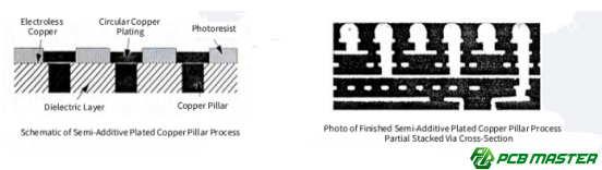
Plated Copper Pillar Process
The plated copper pillar (PCP) process forms solid copper pillars to connect layers.
Advantages: Solid pillars eliminate voids and ensure reliable vertical interconnections.
Disadvantages: Circuit-to-dielectric adhesion can be weaker than other methods.
Application Example: PCBMASTER has successfully manufactured ultra-fine 25μm/25μm circuits using PCP, particularly for high-density IC packaging where strong vertical connectivity is critical.
Plated Filled Via Process
This process combines SAP, laser-drilled vias, and electroplating to fill the vias.
Key Technology: Copper pillar formation inside blind vias ensures reliable connections.
Challenges: Adhesion between the plated copper and dielectric is still a concern, requiring careful process optimization.
Practical Use: PCBMASTER applies this method for boards requiring tight via-to-trace alignment and moderate ultra-fine line density.
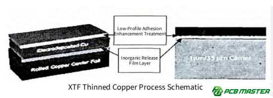
Ultra-Thin Copper (UTC) Process
The UTC process uses specially structured ultra-thin copper foils.
Advantages: Significantly improves adhesion and peeling strength of fine circuits.
Features: Copper thickness and surface structure are precisely controlled to enhance uniformity and reliability.
Applications: Ideal for ultra-fine line substrates where conventional SAP or PCP might suffer delamination. PCBMASTER is exploring UTC for next-generation 10–15μm line substrates.
Semi-Additive Process Type Comparison
SAP Type Key Advantage Limitation / Challenge Typical Application Plated Copper Pillar (PCP) Solid pillars, no voids Lower adhesion to dielectric 25μm/25μm ultra-fine lines, high-density IC packaging Plated Filled Via Combines SAP + laser + plating Adhesion / peeling strength Blind via boards, medium ultra-fine lines Ultra-Thin Copper (UTC) High peeling strength, precise copper structure Higher cost, specialized foil 10–15μm ultra-fine circuits, high-reliability IC substrates
| SAP Type | Key Advantage | Limitation / Challenge | Typical Application |
| Plated Copper Pillar (PCP) | Solid pillars, no voids | Lower adhesion to dielectric | 25μm/25μm ultra-fine lines, high-density IC packaging |
| Plated Filled Via | Combines SAP + laser + plating | Adhesion / peeling strength | Blind via boards, medium ultra-fine lines |
| Ultra-Thin Copper (UTC) | High peeling strength, precise copper structure | Higher cost, specialized foil | 10–15μm ultra-fine circuits, high-reliability IC substrates |
How Does Semi-Additive Pattern Transfer Technology Achieve Fine Circuits?
Semi-additive pattern transfer technology enables the precise formation of ultra-fine circuits by combining advanced imaging and etching techniques. This method allows IC substrate manufacturers to achieve line widths and spacing as small as 10–15μm, ensuring high reliability and performance. PCBMASTER applies these techniques to create high-density, high-precision IC substrates for modern electronics.
How Does Ultra-Fine Line Exposure Technology Work?
Ultra-fine line exposure uses Laser Direct Imaging (LDI) to transfer circuit patterns directly onto a photoresist layer.
l LDI Principle: A laser scans the board surface, exposing only the areas where copper plating is needed. This eliminates masks and improves precision.
l Layer-to-Layer Alignment: LDI ensures each layer aligns correctly, critical for multi-layer IC substrates. Misalignment can cause circuit failures in ultra-fine lines.
l High-End Equipment Capability: Modern LDI machines achieve line widths as small as 10μm with 5–10μm alignment accuracy, enabling the production of ultra-fine, high-density circuits.
For example, PCBMASTER uses LDI to produce 10μm lines for smartphone and high-performance processor substrates, achieving consistent line width and alignment across multiple layers.
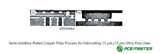
How Does Ultra-Fine Line Rapid Etching Technology Work?
After exposure and copper plating, rapid etching removes unwanted copper while preserving the ultra-fine lines.
l Crystal Defects and Undercut Issues: Chemical copper layers can have microscopic crystal defects. During etching, these defects can cause undercutting, where copper beneath the resist is removed, weakening the line.
l Reducing Copper Thickness and Specialized Etchants: Using thinner plated copper layers and specially formulated etching solutions minimizes undercutting, ensuring precise line profiles.
Practical Example: PCBMASTER successfully produced multi-layer 15μm/15μm circuits using optimized rapid etching. By combining reduced copper thickness, precise etching time, and specialized chemicals, the process achieved high yield and reliable line integrity.
These techniques allow ultra-fine circuits to maintain mechanical strength, signal integrity, and high-density layouts, which are essential for advanced IC packaging.
What Are PCBMASTER’s Advantages and Experiences in Fine Circuit Manufacturing?
PCBMASTER brings years of experience and advanced technology to the production of ultra-fine IC substrate circuits, ensuring high precision, reliability, and yield. Our expertise covers the full spectrum of high-density interconnect (HDI), semi-additive process (SAP), and ultra-thin copper (UTC) manufacturing techniques.
What Equipment and Process Capabilities Does PCBMASTER Offer?
PCBMASTER is equipped with state-of-the-art HDI fabrication lines, semi-additive process plating systems, and ultra-thin copper handling equipment, covering the complete production process for ultra-fine circuits. This enables us to achieve line widths as small as 10μm/10μm while maintaining strict alignment tolerances. By combining high-precision laser direct imaging (LDI) with optimized plating and etching workflows, we ensure that even the most complex, high-density IC substrate designs can be manufactured reliably and consistently.
How Does PCBMASTER Control Yield for Fine Circuits?
Maintaining high yield rates for ultra-fine circuits requires careful control over every production step. PCBMASTER uses low-profile, uniform copper foils, precise copper plating with pulse electroplating, and controlled rapid etching to reduce undercuts and defects. We also employ real-time process monitoring and quality inspection systems to detect deviations early. These strategies allow us to consistently produce high-density 15–25μm circuits with minimal failure rates, ensuring both reliability and cost-effectiveness for our customers.
What Are Some PCBMASTER Service Cases and Customer Applications?
PCBMASTER has successfully supported smartphone, high-performance processor, and advanced automotive IC substrate projects. For example, we produced multi-layer 25μm/25μm circuits for a high-end smartphone substrate, achieving a 98% yield with excellent line uniformity. In another case, our UTC-based process allowed a client to manufacture 10μm ultra-fine circuits for a next-generation processor board, significantly improving adhesion and signal integrity. These examples demonstrate PCBMASTER’s ability to apply advanced fine-line technologies across multiple industries while addressing real-world production challenges.
Conclusion
The production of ultra-fine IC substrate circuits is a complex but essential part of modern electronics. From subtractive methods to semi-additive and ultra-thin copper processes, each technique plays a role in pushing line widths down to 10–25μm while maintaining reliability and yield. Advanced technologies like LDI exposure, pulse electroplating, and rapid etching allow manufacturers to meet the growing demand for high-density, high-performance IC substrates.
As a professional PCB and PCBA supplier, PCBMASTER leverages years of experience, cutting-edge equipment, and optimized process strategies to help engineers achieve precise, high-quality fine circuits. Through careful control of copper thickness, plating, etching, and alignment, we consistently deliver reliable, high-yield products for smartphones, processors, and other advanced applications.
By understanding and applying these advanced fine-line techniques, manufacturers can reduce production risks, improve signal integrity, and meet the ever-increasing demands of next-generation electronics. PCBMASTER remains committed to sharing industry knowledge and providing practical solutions, helping clients stay ahead in the world of ultra-fine IC substrate manufacturing.
FAQs
1. Does reducing line width and spacing in fine circuits affect reliability?
Yes. As line width and spacing decrease, circuits become more susceptible to defects such as short circuits, delamination, and signal integrity issues. Narrow lines are more sensitive to etching irregularities and copper adhesion problems. Advanced processes like semi-additive plating, ultra-thin copper (UTC), and precise laser exposure help maintain reliability even at 10–25μm line widths.
2. How does the cost of the semi-additive process compare to the subtractive method?
The semi-additive process (SAP) is generally more expensive than conventional subtractive etching due to additional steps like electroplating and fine alignment. However, SAP offers higher precision, better yield for ultra-fine circuits, and improved structural reliability, which can offset higher initial costs by reducing defects and production failures in high-density IC substrates.
3. How does ultra-thin copper (UTC) improve substrate peeling strength?
UTC uses specially structured, low-profile copper foils with precise thickness control. This enhances adhesion between copper lines and dielectric layers, significantly reducing the risk of delamination. UTC is especially effective for ultra-fine lines, providing stronger peeling resistance and long-term reliability compared to traditional chemical-deposited copper.
4. What advantages does Laser Direct Imaging (LDI) offer over traditional photolithography?
LDI eliminates masks and uses a laser to directly expose patterns onto photoresist, offering higher line width accuracy, precise layer-to-layer alignment, and reduced defects. Modern LDI systems achieve 10μm line widths with 5–10μm alignment, making them ideal for high-density, multi-layer IC substrates.
5. How does PCBMASTER ensure high yield for 15μm/15μm lines in mass production?
PCBMASTER controls yield through low-profile, uniform copper foils, pulse electroplating, precise LDI exposure, and optimized rapid etching. Real-time process monitoring and quality inspection identify defects early, allowing us to consistently deliver high-yield, ultra-fine circuits for demanding IC substrate applications.

