Power Supply PCB Protection: Key Technologies for Enhanced Safety and Reliability
Power supply PCBs are crucial components in modern electronics, powering devices in industries like electric vehicles (EVs) and medical equipment. They manage the flow of electrical energy, ensuring safe and efficient operation. However, power supply PCBs face challenges like voltage fluctuations, overheating, and electromagnetic interference (EMI), which can lead to device failures and safety risks.
To tackle these issues, advanced protection technologies are now integrated into PCBs. These include AI monitoring, eco-friendly materials, and high-density interconnect (HDI) boards, all designed to improve safety, reliability, and efficiency. These innovations help create more durable and sustainable power supply systems that meet global standards and reduce environmental impact.
This article will explore how these protection technologies enhance power supply PCBs, making them safer, more reliable, and energy-efficient for modern electronics.
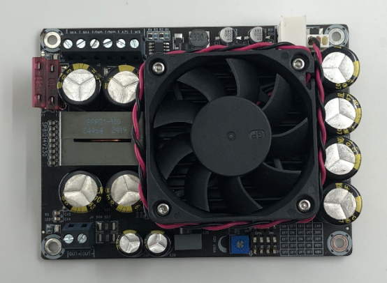
Core Risks Faced by Power Supply PCBs: Why Protection Technologies Matter
Power supply PCBs play a critical role in ensuring that modern devices operate reliably. However, they face several risks that can cause damage to equipment, safety hazards to users, and efficiency problems. To address these challenges, advanced protection technologies are essential.
Reliability Challenges: Avoiding Device Downtime and Failures
Voltage Fluctuations
Even small voltage changes can lead to significant problems for power supply PCBs. For example, a 5% overvoltage can damage capacitors, which are vital for storing and releasing electrical energy. This can also lead to data loss in digital circuits, such as microchips, causing the device to malfunction or shut down unexpectedly. Advanced protection technologies, like overvoltage protection circuits and regulators, are designed to prevent such issues, ensuring the system operates within safe voltage ranges.
EMI
Power supply PCBs use fast-switching components, such as MOSFETs, which can generate EMI. This EMI can disrupt sensitive components like medical sensors or communication systems, affecting the overall performance of the device. Techniques like shielding, grounding, and using common-mode chokes help to reduce EMI and protect the device from potential failure.
Thermal Stress
Excess heat is a major cause of failure in power supply PCBs. For every 10°C increase in temperature, the lifespan of a component is reduced by half. Hotspots caused by narrow traces or crowded layouts can result in early component failure. Thermal management solutions, such as heat sinks, thermal vias, and copper pours, can effectively dissipate heat, keeping the components cool and extending their lifespan.
Safety Risks: Protecting Users and Equipment from Electrical Hazards
Overvoltage and Overcurrent
Excessive voltage or current can cause serious harm to both the device and its users. Overvoltage conditions may lead to electrical fires, while overcurrent can damage components or cause dangerous heating. Using protection components like crowbar circuits, Zener diodes, and resettable fuses ensures that power supply PCBs are protected from these dangerous conditions.
Electric Shock Risks
Power supply PCBs also pose electric shock risks. A fault in the PCB, such as a short circuit or exposed conductive paths, could result in the user being shocked. Ground fault circuit interrupters (GFCIs) and double insulation techniques are commonly used to minimize this risk, providing an extra layer of safety for users.
Fire Hazards
A PCB can catch fire if it is exposed to excessive heat or overcurrent. This is particularly dangerous in high-power applications like electric vehicles or medical devices. To prevent fires, flame-retardant materials (such as FR-4 substrates) are used, along with thermal shutdown sensors that trigger an automatic shutdown if temperatures exceed safe limits.
Efficiency Issues: Reducing Energy Waste
Energy Loss
Inefficient power conversion is a significant issue in many power supply designs. For example, linear power supplies can waste up to 40-70% of the energy as heat. This not only reduces the overall efficiency of the system but also leads to higher energy consumption and increased operational costs.
Efficient Power Conversion
Advanced protection technologies not only help prevent failures but also improve the efficiency of energy conversion. Techniques like using low-ESR capacitors, soft-start circuits, and wide-bandgap semiconductors (such as SiC) help to reduce power loss in switching power supplies (SMPS). These improvements lead to a significant reduction in energy waste, making systems more energy-efficient and cost-effective in the long run.
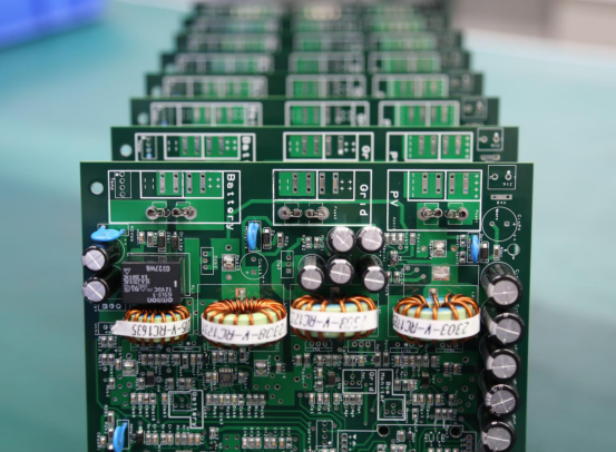
How to Address These Risks with Advanced Protection Technologies?
In order to mitigate the core risks associated with power supply PCBs, advanced protection technologies are essential. These technologies enhance reliability, safety, and efficiency, ensuring that electronic systems work smoothly and safely.
Protection Technologies to Improve Reliability
Electromagnetic Shielding and Grounding
EMI can cause major issues for power supply systems, especially in sensitive applications like medical devices. EMI can disrupt circuits, leading to malfunction or failure. To prevent this, power supply PCBs can use metal enclosures or copper foil shielding. These materials block unwanted electromagnetic waves, creating a protective barrier around the circuit. Additionally, having a low impedance return path through grounding ensures that any EMI is diverted away from sensitive components, improving the system's reliability.
Thermal Management
Heat is one of the main causes of failure in power supply systems. As the temperature increases, components like resistors, capacitors, and integrated circuits (ICs) degrade faster. To combat this, thermal vias (small holes, often around 0.3mm in diameter) are added to the PCB to transfer heat away from critical components. Using copper foil for heat dissipation can also help lower component temperatures, extending the lifespan of the entire power supply system. These thermal management techniques are crucial in systems where high temperatures are common, such as in EVs.
Decoupling Capacitors
In power supply circuits, high-frequency noise can interfere with the proper functioning of ICs and other components. Decoupling capacitors are placed near the power pins of ICs to filter out these high-frequency signals. A typical capacitor value is 0.1µF, which helps smooth the supply voltage and prevents glitches. This simple but effective technique ensures the power supply operates more reliably by reducing noise.
Surface Coatings
Environmental conditions, such as moisture and dust, can damage PCBs, especially in outdoor applications like solar inverters. Polymer coatings are applied to protect the PCB from moisture and dirt. These coatings are waterproof and dustproof, helping the PCB withstand harsh conditions and ensuring long-term reliability in outdoor or industrial environments.
Protection Technologies to Enhance Safety
Overvoltage Protection
Electrical surges or voltage spikes can damage power supply circuits, leading to catastrophic failures. To prevent this, overvoltage clamping circuits, like Zener diodes, are used to limit excessive voltage. When the voltage exceeds a safe threshold, these components redirect the excess voltage away from sensitive parts of the circuit, protecting the system from potential damage.
Overcurrent Protection
Excessive current can lead to overheating, component damage, and even fire. Resettable fuses (also known as polymeric positive temperature coefficient devices) and current-sensing ICs are used to prevent overcurrent situations. These devices automatically disconnect the circuit when the current exceeds safe limits, and they reset after the issue is resolved. This ensures that the system remains safe even during transient current surges.
Electric Shock Protection
Power supply PCBs can pose a risk of electric shock, particularly if there is a fault in the system. GFCIs are integrated to monitor the electrical flow. If an unexpected current is detected, the GFCI immediately disconnects the circuit to protect the user. Additionally, double insulation ensures that users are protected from electrical shock by creating two layers of insulation between the circuit and the user.
Fire Protection
Overheating or overcurrent conditions can cause fires. To prevent this, flame-retardant materials, such as FR-4, are used for the PCB substrate. These materials are specifically designed to resist ignition and prevent fires. Moreover, temperature-sensitive shutdown sensors (set to trigger at 85°C) are integrated into the system to automatically shut down the power supply before it reaches dangerous temperatures, further reducing the risk of fire.
Protection Technologies to Improve Efficiency
Soft-Start Circuits
When a power supply is turned on, a sudden rush of current can cause a surge, potentially damaging components and wasting energy. Soft-start circuits gradually increase the voltage to the system, preventing these sudden current spikes. This technique not only prevents damage to components but also saves 10-15% of the energy required for startup, improving overall system efficiency.
Low-ESR Capacitors
Capacitors with low equivalent series resistance (ESR) are critical in reducing power losses in switching power supplies (SMPS). A typical low-ESR capacitor such as the 100µF/16V X7R type, with an ESR less than 0.1Ω, helps minimize heat generation and energy loss during power conversion. This makes the power supply more efficient and reduces wasted energy.
SiC Devices
Silicon Carbide (SiC) devices offer major advantages over traditional silicon-based components. These devices have lower resistance and can switch at higher frequencies, making them ideal for applications that require efficient power conversion. In systems like EVs and solar power inverters, SiC components can cut energy losses by 50%, significantly improving overall efficiency.
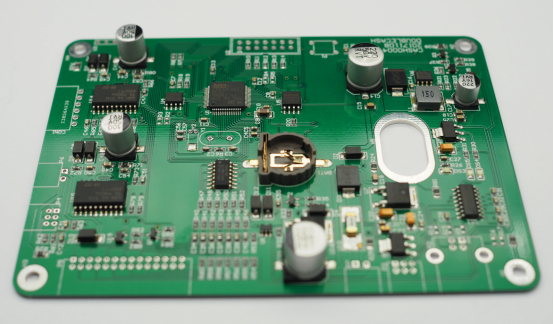
Leading Technologies in Power Supply PCB Protection
Advanced protection technologies in power supply PCBs are revolutionizing the way we approach reliability, safety, and efficiency. From artificial intelligence (AI) monitoring systems to sustainable materials, new innovations are addressing long-standing issues while improving performance. Let's explore some of these cutting-edge technologies.
AI Monitoring: Predicting and Preventing Failures
Defect Detection
AI can help detect defects on power supply PCBs that might be missed by human inspection. By using Convolutional Neural Networks (CNNs), AI analyzes images of PCB surfaces to identify tiny cracks, missing solder points, or misaligned components with up to 95% accuracy. This helps manufacturers catch defects early, improving quality control and reducing product failure rates.
Predictive Maintenance
AI can also predict potential failures before they happen by analyzing data from sensors that monitor temperature and voltage fluctuations. Machine learning models are trained to recognize patterns that indicate impending failures, allowing for early warning alerts. This predictive approach helps prevent unexpected downtime and increases system reliability by addressing issues before they escalate.
Automated Repair
AI-powered robots can perform automatic repairs, such as fixing soldering defects, without human intervention. This automation not only reduces human error but also increases production efficiency by speeding up the repair process. With precise guidance from AI, these robots can ensure repairs are made with high accuracy, leading to better overall PCB quality.
Sustainable Materials: Eco-Friendly Protection
Lead-Free Solder
To meet RoHS (Restriction of Hazardous Substances) standards, many power supply PCBs now use lead-free solder. The most common alternative is SAC305 (an alloy of tin, silver, and copper). This eco-friendly solder offers improved thermal cycling resistance, meaning it performs better over long periods of temperature changes, making it more durable than traditional lead-based solder.
Biodegradable Substrates
For low-power devices like IoT sensors, some manufacturers are turning to biodegradable substrates made from materials like cellulose or hemp. These materials decompose naturally, making them more environmentally friendly than conventional plastic-based PCBs. These substrates are particularly useful in applications where sustainability is a priority.
Recyclable Manufacturing
Designing PCBs for easy disassembly is another key to reducing electronic waste. Manufacturers are increasingly using recyclable copper layers and modular components that can be easily separated and reused at the end of a product's life. This helps reduce the amount of electronic waste generated, supporting a more sustainable manufacturing process.
Green Chemistry
In PCB cleaning processes, many manufacturers are switching to water-based solvents instead of toxic chemicals like acetone. This reduces harmful emissions during the PCB cleaning process, making it safer for workers and more eco-friendly.
HDI Boards: Miniaturization and Stronger Protection
Micro-Hole Technology
HDI PCBs use advanced micro-hole technology, such as blind and buried vias, with hole diameters of just 6-8 mils. These tiny holes allow for more compact component layouts and reduced EMI. The compact design helps optimize the overall size of the power supply system while improving its performance.
Fine Pitch Routing
Using 2mil (50µm) fine pitch routing reduces the distance between signal paths, which minimizes heat buildup and reduces electrical losses. The reduced signal path length also improves signal integrity, ensuring reliable data transmission within the system.
Thermal Management
HDI boards are equipped with advanced thermal vias and copper foil designs to better manage heat dissipation. This allows high-power HDI boards to maintain low temperatures, increasing their overall reliability and ensuring that they perform optimally in demanding applications, such as EV power systems.
Flexible PCBs: Protection in Dynamic Environments
Durability
Flexible PCBs made from materials like polyimide are highly durable, capable of withstanding over 100,000 bending cycles. This makes them ideal for applications in dynamic environments, such as automotive airbags or foldable smartphones, where the PCB must maintain its integrity despite constant movement.
Lightweight Design
Compared to traditional rigid PCBs, flexible PCBs are approximately 30% lighter, making them an excellent choice for aerospace and electric vehicle applications, where weight reduction is a critical factor for performance and energy efficiency.
Moisture Resistance
Polyester coatings on flexible PCBs provide superior moisture resistance, ensuring the PCB remains functional even in wet or humid conditions. This is particularly important for medical devices like endoscopes and marine electronics, where moisture protection is a key concern.
SiC Devices: High-Temperature and High-Voltage Protection
Temperature Tolerance
SiC devices can operate at temperatures up to 175°C, significantly reducing the need for cooling systems. This makes them suitable for high-power applications such as EV inverters, where traditional components might overheat. With SiC, power supplies can run more efficiently, cutting down on cooling costs and energy consumption.
High Voltage Handling
SiC components have a breakdown voltage of up to 1700V, making them ideal for 800V EV inverters. By handling high voltages efficiently, SiC devices reduce energy losses by 50%, providing a significant improvement in system efficiency. This makes them a top choice for electric vehicle manufacturers looking to enhance the performance of their power systems.
Low On-Resistance
SiC MOSFETs feature low on-resistance (as low as 28mΩ), which helps minimize power losses in high-current circuits. This characteristic is particularly beneficial for reducing heat and improving the overall efficiency of systems like electric vehicles or renewable energy systems that rely on high-efficiency power conversion.
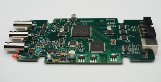
Benefits of Protection Technologies: Enhancing Safety, Reliability, and Efficiency
In modern power supply systems, protection technologies play a crucial role in improving safety, reliability, and efficiency. By addressing key issues such as voltage surges, electrical faults, and energy waste, these technologies ensure that systems run smoothly and safely. Let’s dive into how these protection technologies bring tangible benefits.
Enhancing Safety
Transient Voltage Suppressors (TVS)
A TVS is designed to protect sensitive components from voltage surges. For example, a TVS can limit a 1000V surge down to just 50V, preventing damage to microchips and other vulnerable parts. This protection is essential for preventing system failures caused by unexpected voltage spikes, especially in devices like medical equipment or automotive electronics.
GFCI
GFCI provide safety by quickly detecting electrical faults and disconnecting the power within 10 milliseconds. This is particularly important for preventing electrical shocks. For instance, in household power systems or medical devices, a GFCI can protect users from potentially deadly electrical hazards by cutting off the power before a fatal shock occurs.
Flame-Retardant Design
Using materials that meet the UL 94 V-0 standard, which is a fire-resistant rating, ensures that power supply PCBs are safer. For instance, in electric vehicle (EV) PCBs, these flame-retardant materials help prevent fires from spreading in case of a short circuit or overheating. This reduces the risk of fire damage to the vehicle or the people using it.
Enhancing Reliability
AI Predictive Maintenance
AI technology can be used to monitor power supply systems and predict failures before they happen. In data centers, for example, AI-driven predictive maintenance can reduce unplanned downtime by 40%. By analyzing sensor data such as temperature, voltage, and current, AI can predict component wear and tear, allowing for timely repairs or replacements. This significantly improves the reliability and availability of critical systems.
HDI Thermal Via Design
HDI boards incorporate thermal vias that help dissipate heat more effectively. In high-power applications, like those found in electric vehicles, this technology can reduce the temperature of sensitive components by up to 25°C, thus preventing overheating and extending the lifespan of components. Effective thermal management is essential for maintaining the reliability of high-performance power supplies.
Surface Coatings
To protect outdoor devices from environmental conditions, moisture-resistant surface coatings are used. These coatings reduce the failure rate of outdoor equipment such as solar inverters by up to 60%. For example, in solar power systems, these coatings ensure that the components stay functional even when exposed to rain or high humidity.
Enhancing Efficiency
SiC Inverters
SiC inverters are increasingly used in EVs because they improve energy conversion efficiency. In an EV system, SiC inverters can achieve 99% efficiency, compared to traditional silicon-based systems, which only reach about 89%. This 10% increase in efficiency means that for every 100 kilometers driven, an EV with a SiC inverter saves about 5 kWh of energy, extending the vehicle's driving range and reducing overall energy consumption.
BridgeSwitch2 Integrated Circuits
The BridgeSwitch2 IC is a new type of integrated circuit that eliminates the need for shunt resistors in inverter systems, leading to a 3% improvement in efficiency. Additionally, it allows for 30% reduction in PCB space, which makes it especially useful in designs where space is limited, such as in compact power supply systems or portable devices.
Soft-Start Circuits
A soft-start circuit helps reduce the impact of high inrush current when a device is powered on. By smoothing the initial voltage increase, these circuits prevent sudden spikes in current, which can damage components and waste energy. For example, a soft-start circuit can reduce startup current by 70%, which translates into energy savings during the startup phase of devices like motors or power supply units.
Challenges in Implementing Power Supply PCB Protection Technologies
While advanced protection technologies offer numerous benefits, integrating them into power supply PCBs presents several challenges. These challenges primarily revolve around technical complexity and cost.
Complexity of Technology Integration
EMI Crosstalk
EMI can be a significant challenge in power supply PCBs, especially with components like AI sensors and SiC MOSFETs. These components can generate unwanted electrical noise that may interfere with other sensitive circuits. To address this issue, a common solution is to separate the analog and digital ground planes within the PCB. This ensures that noise generated by high-power circuits, such as switching components, doesn’t affect sensitive analog circuits like sensors. Additionally, EMI filters can be added to further reduce noise, improving the overall performance of the PCB. This solution helps minimize the impact of crosstalk between circuits, ensuring the system works efficiently and without interference.
Thermal Management Requirements
In high-power applications, managing heat is critical to prevent overheating and component failure. Power supply systems that involve high currents or rapid switching, like those in EVs, generate a lot of heat. To prevent damage, accurate thermal simulation tools are required during the design phase. These tools help predict potential heat buildup in different parts of the PCB and allow for the design of adequate cooling solutions such as heat sinks or thermal vias. Without proper thermal management, components can overheat, leading to system failures and reduced reliability.
Cost Barriers
High-Cost Materials
One of the biggest barriers to adopting advanced protection technologies in PCBs is the high cost of materials. For example, SiC devices, known for their superior performance in high-voltage and high-temperature applications, are significantly more expensive than traditional silicon-based components. Similarly, HDI boards, which allow for more compact and efficient designs, use specialized materials that are also costly. While these materials offer better performance and longer lifespan, their higher upfront cost can be a significant factor for manufacturers when choosing between conventional and advanced designs. The decision often involves weighing the long-term benefits of reliability and efficiency against the initial investment required.
Manufacturing Complexity
Manufacturing high-density PCBs, particularly those with HDI features, presents challenges in terms of precision and quality control. HDI boards require smaller vias, fine pitch components, and advanced soldering techniques to ensure that everything functions properly. Achieving this level of precision often demands advanced machinery and processes, which can drive up production costs. Additionally, the complexity of assembling HDI boards may increase the likelihood of manufacturing defects, which can further increase costs due to the need for additional testing and rework. As the demand for more compact and efficient systems increases, manufacturers need to balance cost with the advantages of these high-performance designs.
Conclusion: The Future of Power Supply PCB Protection
The future of power supply PCB protection is being shaped by key trends such as the integration of advanced protection technologies like AI monitoring, sustainable materials, and HDI. These innovations are transforming how power supply systems handle challenges like voltage fluctuations, overheating, and EMI. As the demand for smarter, more reliable electronics grows, the need for continued innovation in PCB protection becomes even more critical.
By adopting cutting-edge solutions, such as SiC devices for high-voltage applications and AI-driven predictive maintenance, the industry can significantly improve the safety, reliability, and efficiency of power supply systems. These advancements will not only ensure safer devices but also make them more energy-efficient and long-lasting.
As we move forward, the integration of these advanced technologies will be essential for creating the next generation of safe, reliable, and efficient electronic systems. If you're interested in learning more about PCB technology or need assistance with your own designs, PCBMASTER is here to help with professional advice and support.
FAQs
How does AI monitoring improve the defect detection process in power supply PCBs?
AI monitoring significantly enhances the defect detection process in power supply PCBs by using advanced machine learning techniques to identify issues that may be difficult for the human eye to spot. One of the key methods is Convolutional Neural Networks (CNNs), which analyze PCB images to detect micro-cracks, missing solder joints, or misaligned components. These AI systems can achieve up to 95% accuracy in identifying defects, reducing the risk of faulty boards being shipped to production. By integrating AI into the monitoring process, manufacturers can detect issues early in the production cycle, preventing costly mistakes and ensuring that only high-quality PCBs make it to the next stage.
What are the benefits of using SiC devices in power supply PCB designs?
SiC devices offer significant advantages in power supply PCB designs, especially for high-power applications. One of the key benefits is higher efficiency, as SiC components can operate at higher voltages (up to 1700V) and temperatures (up to 175°C) than traditional silicon devices. This results in lower energy losses and a reduced need for extensive cooling systems. SiC devices also have lower on-resistance, which reduces power dissipation, improving overall system efficiency. They are ideal for applications such as EV inverters and solar power systems, where high efficiency and compact size are critical.
Can HDI boards handle high-power systems without compromising performance?
Yes, HDI boards are specifically designed to handle high-power systems without compromising performance. HDI boards utilize microvia technology, which allows for more compact and efficient component layouts. This enables shorter signal paths, reducing EMI and heat generation. Additionally, thermal management solutions like heat vias and copper heat sinks are integrated into the design to manage the high thermal loads generated by high-power components. As a result, HDI boards can maintain high performance while managing power efficiently, making them suitable for demanding applications like power supplies for EVs or industrial machinery.
How does spread spectrum technology help in reducing EMI in power supply PCBs?
Spread spectrum technology helps reduce EMI in power supply PCBs by spreading the frequency of the signal over a wide range. This makes the emissions from the PCB less concentrated at a single frequency, thereby reducing the chance of interference with nearby electronic systems. By using modulation techniques to slightly vary the frequency, the energy from the signal is dispersed across a broader spectrum, making it less likely to cause interference with other sensitive devices. This is especially important in designs where strict EMI standards must be met, such as in medical equipment, automotive electronics, and telecommunication devices.
What are the environmental benefits of using bio-based substrates and lead-free solders in PCB manufacturing?
Using bio-based substrates and lead-free solders in PCB manufacturing offers substantial environmental benefits. Bio-based substrates, made from degradable materials like cellulose or hemp, are an eco-friendly alternative to traditional petroleum-based PCB materials. These substrates are biodegradable and can reduce the amount of electronic waste, contributing to more sustainable electronics. Additionally, switching to lead-free solders, such as SAC305 (a tin-silver-copper alloy), eliminates the environmental and health hazards associated with lead. Lead-free solders are also more durable and perform better under thermal cycling, contributing to longer-lasting products. Overall, these sustainable materials help reduce the carbon footprint of PCB manufacturing, aligning with global efforts to promote green electronics.
Author Bio
Hi, I'm Carol, the Overseas Marketing Manager at PCBMASTER, where I focus on expanding international markets and researching PCB and PCBA solutions. Since 2020, I've been deeply involved in helping our company collaborate with global clients, addressing their technical and production needs in the PCB and PCBA sectors. Over these years, I've gained extensive experience and developed a deeper understanding of industry trends, challenges, and technological innovations.
Outside of work, I'm passionate about writing and enjoy sharing industry insights, market developments, and practical tips through my blog. I hope my posts can help you better understand the PCB and PCBA industries and maybe even offer some valuable takeaways. Of course, if you have any thoughts or questions, feel free to leave a comment below—I'd love to hear from you and discuss further!