


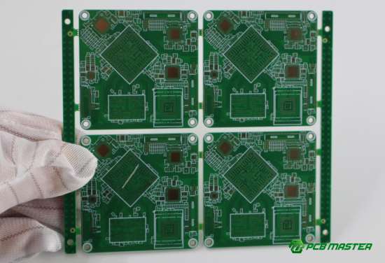
Essential Parts of a PCB: Functions and Importance Explained
A PCB, or Printed Circuit Board, is a key component in nearly all electronic devices. It provides a platform where various electronic components like resistors, capacitors, and chips are placed and connected to create a working circuit. Without PCBs, everyday devices such as smartphones, computers, and medical equipment would not function. Understanding the different parts of a PCB is essential for anyone involved in electronics design or manufacturing. Each part plays a crucial role in ensuring that the device is reliable, performs efficiently, and lasts over time. For instance, copper traces on a PCB allow electrical signals to pass between components, while the solder mask protects the copper from damage. Knowing how these parts work together can help in creating more effective, durable, and efficient products. As technology continues to evolve, understanding PCBs remains vital in ensuring the success of electronic devices.
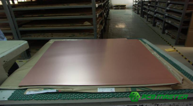
Substrate (Base Material) of a PCB
The substrate is the foundational material that makes up the core structure of a PCB. It is typically made from insulating materials like FR-4, CEM1, or flexible substrates. The substrate provides both mechanical support and electrical insulation, ensuring that all components and copper traces are securely mounted and do not short-circuit each other.
Importance of the Substrate
l Supporting Circuit Components: The substrate holds all the components of the PCB, such as resistors, capacitors, and chips, in place. It ensures the board maintains its structural integrity, even during manufacturing and long-term use. A strong substrate prevents flexing or warping of the board, which can disrupt connections.
l Electrical Insulation: One of the most critical roles of the substrate is to prevent electrical shorts. Materials like FR-4 are highly effective at providing electrical insulation, ensuring that electrical currents only travel through the designated copper paths. This helps the PCB function without unintended interference between components.
l Thermal Management: Substrates made from high-quality materials not only insulate but also help in heat dissipation. When components generate heat, the substrate helps spread it evenly, preventing the board from overheating and damaging sensitive components. For example, FR-4 has a good balance of heat resistance and thermal conductivity, making it ideal for many common applications.
Common Substrate Materials
l FR-4: This is the most widely used substrate material for PCBs. It is made from woven fiberglass and epoxy resin, providing excellent mechanical strength, electrical insulation, and heat stability. FR-4 is used in most consumer electronics, including computers, smartphones, and televisions.
l CEM1 and CEM3: These are more affordable alternatives to FR-4. They are used in low-cost applications where high-performance is not critical. CEM1 is a paper-based material, while CEM3 uses a composite of fiberglass and resin. These materials are typically found in simpler, cost-sensitive devices like basic home appliances.
l Flexible Substrate: For applications that require bending or conforming to complex shapes, flexible substrates are used. These are commonly found in devices like smartphones and wearables, where the PCB needs to be flexible and lightweight, such as in curved displays or compact designs. Flexible substrates can be made from materials like polyimide.
Copper Traces on a PCB
Copper traces are the main pathways on a PCB through which electrical signals and current flow. These thin copper lines connect various electronic components, such as resistors, capacitors, and chips, allowing them to communicate and function together as part of a circuit. Copper is chosen for these traces because of its excellent electrical conductivity, making it ideal for transmitting power and signals efficiently across the board.
Why Are Copper Traces Important?
l Current Transmission: Copper traces provide the necessary paths for electrical current to flow from one component to another. If these traces are not properly designed, the electrical signals can experience interference, or the current may be restricted. This can result in malfunctioning circuits, power loss, or even total failure of the device.
l Electrical Design: The design of copper traces directly influences the performance of the PCB. Factors such as trace width and layout affect the impedance, signal integrity, and overall power distribution of the circuit. Proper trace design ensures that the electrical signals remain clear and accurate, and the circuit operates at peak performance.
l Thermal Management: Copper's thermal conductivity helps dissipate heat generated by the electrical current. As current flows through the traces, heat is naturally produced. The copper traces help spread this heat across the board, preventing overheating and ensuring the components remain within safe operating temperatures.
Key Design Considerations for Copper Traces
l Trace Width: The width of the copper trace is critical. If the trace is too narrow, it may overheat due to excessive current flow, causing damage or circuit failure. If the trace is too wide, it takes up unnecessary space on the PCB, reducing the overall design density and efficiency. Proper calculation of trace width is essential for optimal performance and safety.
l Routing Optimization: The layout of the copper traces is just as important as their width. Efficient trace routing minimizes the distance between components and reduces signal loss or interference. In high-speed circuits, signal integrity is vital, so careful placement of traces is necessary to avoid crosstalk and noise, which can distort data transmission.
l High-Speed Signal Considerations: For designs that involve high-frequency or high-speed signals, such as in computers or communications equipment, the layout of copper traces becomes even more important. The impedance of the trace must be carefully managed, and the traces should be kept as short and direct as possible to prevent signal degradation.
Real-Life Example:
In a smartphone PCB, copper traces connect the various chips (e.g., processor, memory, sensors) and components. If the trace design is not optimal, the signal between the chips may degrade, leading to slower performance or even system crashes. This is why smartphone manufacturers carefully design their PCBs, ensuring copper traces are wide enough to handle current without overheating, while also keeping them compact for efficient signal flow.
Solder Mask on a PCB
A solder mask is a thin layer of protective material applied to the surface of a PCB. Typically green, but sometimes in other colors, the solder mask serves several important functions in protecting the PCB during and after the manufacturing process. It prevents excess solder from creating unwanted connections between copper traces, which could lead to short circuits or other electrical failures.
Why Is the Solder Mask Important?
l Prevents Short Circuits: During the soldering process, excess solder can unintentionally bridge connections between different copper traces. This can cause short circuits, leading to faulty performance or complete failure of the circuit. The solder mask prevents this by covering the copper traces and leaving only the necessary areas exposed for soldering components.
l Protects Copper Layers: The solder mask also shields the copper traces from environmental damage. Factors like moisture, dust, and corrosion can degrade copper over time, affecting the performance and lifespan of the PCB. The solder mask provides a protective barrier, ensuring the copper remains intact and functional for longer periods.
l Increases Reliability: By protecting both the copper traces and components from external environmental factors, the solder mask helps improve the overall reliability of the PCB. It reduces the chances of corrosion or physical damage, making the device more durable and less prone to failure.
Common Issues with Solder Masks
l Peeling or Scratching: One of the biggest issues with solder masks is peeling or scratching. If the solder mask layer is damaged, the copper traces underneath become exposed. This can lead to contamination, corrosion, or damage to the PCB, reducing its performance and lifespan. For example, if a PCB is exposed to moisture, the copper traces can oxidize, causing electrical issues.
l Design Challenges: Applying the solder mask requires precision, especially around small or complex areas of the PCB. The design needs to ensure that the mask does not overlap with areas where components need to be soldered. Any inaccuracies in the solder mask design can result in incomplete protection or difficulty during assembly, leading to production delays or costly errors.
Real-Life Example:
Consider the PCB of a smartphone. The small, tightly packed components and traces require precise soldering. If the solder mask did not cover the right areas or if it were damaged, excess solder could easily cause short circuits between tiny traces, making the phone malfunction. By ensuring the solder mask is properly applied, manufacturers protect the delicate components and maintain the phone's reliability.
Silkscreen Layer on a PCB
The silkscreen layer is a printed layer on the surface of a PCB that is used to mark the positions of components, labels, and other important information. It is typically applied using white ink, but other colors may also be used depending on the design. This layer plays a crucial role in the assembly and maintenance of electronic devices by making the PCB easier to read and understand.
Why Is the Silkscreen Layer Important?
l Component Identification: One of the main functions of the silkscreen layer is to label the positions and designations of the components on the PCB. These markings help engineers, technicians, and assembly workers easily locate and identify each component during the assembly process. This reduces the chances of mistakes, like placing a component in the wrong spot, which can result in faulty circuits.
l Troubleshooting and Repair: For maintenance and repair, the silkscreen layer is an invaluable tool. It provides essential information that helps technicians identify faulty components quickly. Without this layer, it would be difficult to trace and diagnose problems, especially in complex circuit boards with many components.
l Improves Readability: In complex or high-density PCB designs, the silkscreen layer improves the readability of the board. By clearly marking the locations and functions of each component, it makes it easier to understand the overall circuit layout, reducing the likelihood of errors during manufacturing and future repairs.
Design Considerations for the Silkscreen Layer
l Clear and Legible Information: It is important that the text and symbols on the silkscreen layer are clear and easy to read. This includes selecting the appropriate font, size, and spacing for the labels. In highly compact or micro-sized designs, where space is limited, the silkscreen must still be legible to ensure proper assembly and debugging.
l Avoiding Coverage of Component Pins: The silkscreen layer should never overlap the pins of components. If it does, it could obstruct the placement of solder or make it difficult to establish proper connections. This could lead to poor solder joints or even failure to solder certain components, affecting the overall functionality of the PCB.
Real-Life Example:
In a home appliance PCB, the silkscreen layer clearly marks where each component such as capacitors, resistors, and microcontrollers should be placed. If the assembly team misplaces a component, the circuit may fail, causing the appliance to malfunction. The silkscreen also provides labels for the technicians, allowing them to easily spot and replace faulty components when needed, saving time and improving efficiency during repairs.
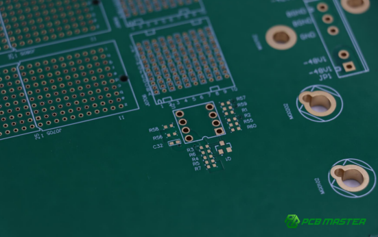
Pads and Vias on a PCB
Pads and vias are two essential components of a PCB that help ensure the circuit board functions properly. Pads are used to attach electronic components by soldering, while vias are tiny holes that create electrical connections between different layers of the PCB.
Why Are Pads and Vias Important?
l Pads – Soldering Points: Pads are the areas where components are attached to the PCB. These small, flat areas are designed to be coated with solder, allowing components like resistors, capacitors, and chips to be securely fixed in place. Pads must be sized and positioned correctly to ensure proper electrical connections, which are essential for the overall functionality of the PCB.
l Vias – Layer-to-Layer Connection: Vias are small holes drilled into the PCB that connect different layers of the board. In multi-layer PCBs, vias are critical for transmitting electrical signals and power between layers. Without vias, it would be impossible to create complex multi-layer circuits, which are common in advanced electronic devices like smartphones and computers.
Common Types of Vias
l Blind Vias: Blind vias connect the outermost layers of the PCB to one or more inner layers but do not extend through the entire board. These vias are useful for designs where components need to be connected across different layers without the need for holes that reach the board’s surface.
l Buried Vias: Buried vias are entirely internal, meaning they connect two or more inner layers but do not pass through to the outer layers of the PCB. This type is often used in complex, high-density designs where space optimization is crucial.
l Micro Vias: Micro vias are very small holes typically used in high-density interconnect (HDI) PCBs. These vias are used for advanced electronics where the size of the PCB is minimized, and more layers are required for increased functionality, such as in mobile phones or wearable technology.
Real-Life Example:
In a smartphone PCB, pads are used to attach the tiny components like resistors, capacitors, and microchips. The vias, particularly blind vias, ensure that signals can travel from the top layer, where the components are soldered, to the inner layers where other circuitry and power planes are located. This inter-layer connection is crucial for the phone’s performance, enabling it to run multiple applications, process data, and communicate with other devices.
Conclusion
The essential components of a PCB—such as the substrate, copper traces, solder mask, silkscreen, and pads/vias—each play a crucial role in ensuring the board’s functionality, performance, and longevity. Careful attention to factors like material selection, trace layout, and layer connections is vital to creating a stable, reliable, and efficient circuit board. Whether it's optimizing the copper traces for minimal interference, ensuring the proper application of the solder mask, or designing accurate pads for secure soldering, every detail impacts the performance of the final product.
For businesses looking to design high-quality PCBs, partnering with an experienced manufacturer is key. PCBMASTER, a trusted supplier of PCBs and PCBA services, offers years of expertise in creating custom solutions tailored to your specific needs. Whether you're designing for consumer electronics, medical devices, or complex industrial applications, PCBMASTER’s commitment to precision and quality ensures that your products will meet the highest standards for reliability and performance.
FAQs
1. Why is the choice of substrate material crucial for a PCB?
The choice of substrate material is critical because it directly affects electrical isolation, mechanical strength, and thermal management. The right substrate ensures that the circuit operates reliably and maintains stability. For example, FR4 provides strong insulation, excellent mechanical properties, and good thermal resistance, making it a popular choice. A poor substrate choice could lead to electrical shorts, physical damage, or overheating, compromising the PCB’s overall performance.
2. Does the design of copper traces impact PCB performance?
Yes, the design of copper traces plays a significant role in PCB performance. The width and layout of copper traces directly affect signal transmission speed, noise levels, and current loss. Optimizing the design of copper traces helps maintain signal integrity and reduces electromagnetic interference (EMI). For high-speed or high-frequency applications, ensuring the right trace width and proper routing is essential to ensure efficient performance and prevent signal degradation.
3. How can the integrity of the solder mask be maintained?
To ensure the integrity of the solder mask, it must be designed to avoid excessive coverage and ensure it is protected from physical or chemical damage. The solder mask should only cover areas that do not require soldering and should leave exposed pads or vias clear. Additionally, it should be resistant to external factors like moisture and abrasion, which can cause degradation. A well-applied solder mask ensures long-term electrical protection and prevents solder bridges, contributing to the board’s durability.
4. What is the practical purpose of the silkscreen layer?
The silkscreen layer provides essential markings for the components on the PCB, helping identify their positions, part numbers, and functions. During assembly, testing, and maintenance, the silkscreen layer serves as a guide for engineers and technicians, reducing errors. It also aids in troubleshooting by providing clear labels for each component, improving repair efficiency and reducing downtime when components need replacement or testing.
5. How is heat managed in a PCB?
Heat management in a PCB is achieved through thoughtful design choices like placing heat dissipation holes, selecting thermally conductive materials, and planning heat paths. By optimizing the layout to direct heat away from sensitive components and using materials that dissipate heat effectively, the risk of overheating is minimized. This ensures that components remain within their safe operating temperature range, improving the PCB’s overall performance and longevity.

