


PCB Fiberglass Cloth Types and Differences: E-Glass vs. NE-Glass vs. T-Glass vs. Quartz
As data rates increase and packaging structures become more complex, PCB material selection directly affects electrical performance and reliability. The reinforcement layer inside the laminate has a measurable impact on signal transmission, dielectric loss, thermal expansion behavior, and dimensional stability.
Fiberglass cloth is a key structural component in PCB substrates. Differences in glass composition, thickness specification, and weaving technology lead to clear variations in dielectric constant, loss factor, CTE, and processing characteristics. Choosing the appropriate glass cloth is therefore essential for high-speed, high-frequency, and advanced packaging applications.
What Is Fiberglass Cloth in PCB Substrates and What Role Does It Play?
Fiberglass cloth is the reinforcing material inside PCB laminates. It provides mechanical strength, controls thermal expansion, and strongly influences electrical performance.
Where Is Fiberglass Cloth Located in FR-4 and Advanced PCB Laminates?
Fiberglass cloth sits between resin layers, forming a composite structure that becomes the rigid core of the PCB.
Resin + Fiberglass Cloth + Filler Composite Structure
A standard PCB base material such as FR-4 is a composite. It is made of epoxy resin, woven fiberglass cloth, and sometimes inorganic fillers.
- The resin bonds everything together.
- The fiberglass cloth provides structural reinforcement.
- The fillers help fine-tune thermal and dielectric properties.
When heat and pressure are applied during lamination, resin flows into the gaps of the glass fabric and cures into a solid sheet. This sheet becomes the PCB core or prepreg layer.
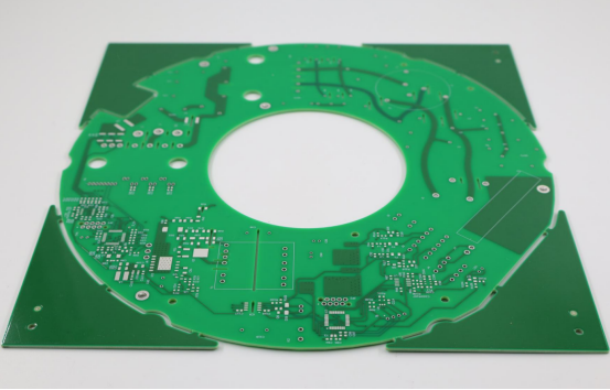
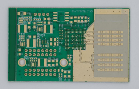
For example, in a 6-layer server motherboard, multiple sheets of resin-impregnated fiberglass cloth (prepreg) are stacked and pressed to form a stable multilayer structure.
Fiberglass Cloth as a Structural Reinforcement Material
Fiberglass cloth acts like a framework inside the laminate. Without it, cured resin alone would be brittle and dimensionally unstable.
The woven glass fibers:
- Increase tensile strength
- Prevent cracking during drilling and routing
- Maintain dimensional stability during thermal cycling
In high-layer-count PCBs, such as data center switches, this reinforcement prevents panel distortion during repeated reflow soldering cycles.
How Does Fiberglass Cloth Directly Affect PCB Performance?
Fiberglass cloth influences mechanical strength, dielectric properties (Dk and Df), and thermal expansion (CTE), which directly impact signal quality and reliability.
Mechanical Strength and Dimensional Stability
Fiberglass significantly improves bending strength and rigidity. This is critical for large PCBs, such as telecom backplanes, where board warpage can cause assembly problems.
It also controls X-Y shrinkage during lamination. If dimensional stability is poor, via alignment may shift, leading to registration defects in multilayer boards.
In simple terms, the glass fabric helps the board “stay in shape” under heat and mechanical stress.
Dielectric Properties (Dk and Df)
The glass composition directly affects dielectric constant (Dk) and dissipation factor (Df).
- Dk (dielectric constant) affects signal speed. Lower Dk means faster signal propagation.
- Df (dissipation factor)affects signal loss. Lower Df means less energy lost as heat at high frequency.
For example, E-glass typically has higher Dk and Df than low-loss glass types. In high-speed digital PCB design, this difference can increase insertion loss at 56G or 112G data rates.
In short, fiberglass cloth is not electrically neutral. It directly shapes high-frequency signal behavior.
Coefficient of Thermal Expansion (CTE) Matching
CTE describes how much a material expands when heated.
Silicon chips have very low CTE. If the PCB substrate expands too much during reflow soldering, stress builds at solder joints.
Low-CTE fiberglass types (such as T-glass) reduce mismatch between the PCB and the chip. This improves solder joint fatigue life in applications like AI processors or high-end CPUs.
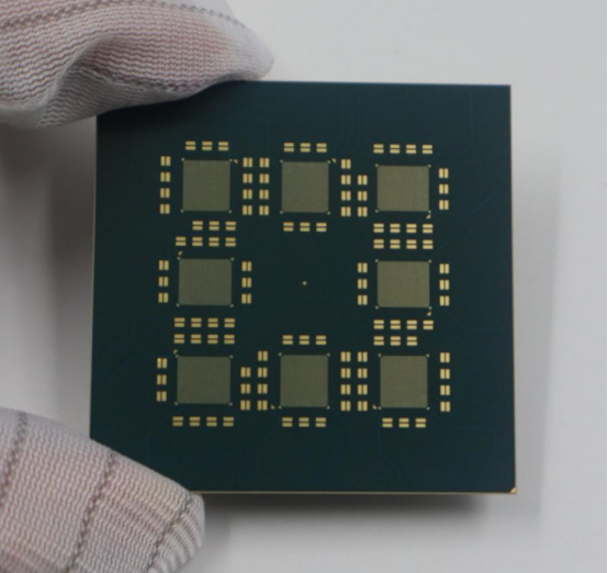
This is especially important in BGA and FC-BGA packaging, where hundreds or thousands of solder balls must remain reliable.
Why Must High-Speed and High-Frequency PCBs Carefully Select Fiberglass Cloth?
Because at high data rates and high frequencies, small material differences create measurable signal loss, timing errors, and reliability risks.
Higher Signal Integrity Requirements
As data rates increase to 56G, 112G, and even 224G PAM4 signaling, signal margins become very small.
Variations in fiberglass weave create local dielectric differences. This can cause skew in differential pairs, a phenomenon known as the “fiber weave effect.”
At low speeds, this effect is negligible. At 112G, it can cause measurable eye diagram degradation.
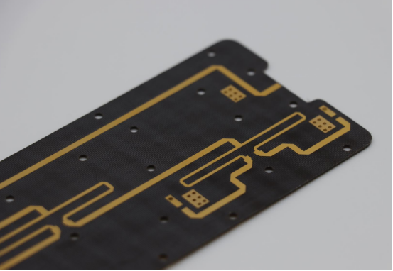
Therefore, advanced PCBs use spread glass or flattened yarn to reduce dielectric variation.
Packaging Warpage and Reliability Challenges
Modern AI accelerators and networking ASICs generate high heat and use large BGA footprints.
If the substrate CTE is too high, repeated thermal cycling causes:
- Warpage
- Solder fatigue
- Cracked interconnects
Choosing the correct fiberglass type helps balance mechanical stiffness and thermal expansion, reducing long-term failure risk.
Trend Toward ≥56G / 112G / 224G High-Speed Design
The industry trend is clear: bandwidth is increasing every generation.
- 56G SERDES became common in data centers.
- 112G is now mainstream for high-end networking equipment.
- 224G development is underway for next-generation switches.
At these speeds, laminate material selection is part of signal design, not just mechanical design. Fiberglass type, glass style (e.g., 7628 vs. 1035), and weave technology all become electrical design parameters.
In summary, as speed increases, fiberglass cloth moves from being a background material to a performance-critical design variable.
What Are the Different Types of Fiberglass Cloth in PCBs Based on Glass Composition, and What Are Their Performance Differences?
Fiberglass cloth used in PCBs varies in its glass composition, and each type offers distinct performance characteristics such as dielectric constant (Dk), dissipation factor (Df), and thermal expansion (CTE). These differences make certain fiberglass types more suitable for specific applications.
What Are the Characteristics of E-glass Fiberglass Cloth, and What Applications Is It Suitable For?
E-glass is the most common and cost-effective type of fiberglass, suitable for standard PCB applications but with higher signal loss and thermal expansion.
- Dk (Dielectric Constant): E-glass has a Dk around 6-7 at 1 MHz, which means it has a higher dielectric constant compared to specialized glass types.
- Df (Dissipation Factor): The dissipation factor is relatively high, meaning more signal energy is lost as heat, which is less ideal for high-speed circuits.
- CTE (Coefficient of Thermal Expansion): E-glass has a standard CTE, which works for most consumer electronics but may not be ideal for high-end chips or high-reliability systems.
Typical Applications:
- Standard FR-4 boards: Used in most consumer electronics and low-cost PCBs like power supplies.
- Multilayer PCBs: Ideal for mid-range applications that don’t require ultra-low loss or precise thermal expansion.
Example: E-glass is often used in everyday electronics such as smartphones and home appliances, where high-speed signal transmission and extreme reliability aren’t top priorities.
What Are the Advantages of NE-glass / L-glass Fiberglass Cloth?
NE-glass and L-glass offer lower dielectric constants and dissipation factors compared to E-glass, making them ideal for high-speed, high-performance applications.
- Dk (Dielectric Constant): NE-glass and L-glass have a lower Dk, ranging from 3.5 to 4.3, which results in faster signal transmission.
- Df (Dissipation Factor): The Df for NE-glass is lower (about 0.0015 to 0.002), meaning less signal loss and better signal integrity.
- CTE (Coefficient of Thermal Expansion): NE-glass and L-glass have a lower CTE, improving thermal stability and reducing the risk of warpage in high-end PCBs.
Typical Applications:
- Server motherboards: Requires low Dk for better high-speed signal integrity.
- 5G base stations: Demands low loss for efficient signal propagation.
- High-speed digital boards: Ideal for applications where data integrity at high frequencies is crucial.
Example: L-glass is used in telecom and server boards, where low signal loss and high reliability are essential for handling large amounts of data.
Why Is T-glass Suitable for High-End Packaging Boards?
T-glass provides ultra-low Dk, low Df, and a very low CTE, making it ideal for advanced packaging applications that require high signal integrity and minimal thermal expansion.
- Dk (Dielectric Constant): T-glass has a very low Dk, which improves signal transmission speed by reducing the electrical path’s delay.
- Df (Dissipation Factor): T-glass has a low Df, ensuring minimal signal loss, which is critical for high-frequency and high-speed applications.
- CTE (Coefficient of Thermal Expansion): With a CTE ≤3.0 ppm/°C, T-glass matches closely with the thermal expansion of silicon chips, reducing thermal stress during operation.
Typical Applications:
- AI GPU and CPU FC-BGA packages: Ensures stable electrical performance under high temperatures and fast processing.
- High-performance computing (HPC) boards: Used in environments where high-speed signals and thermal management are critical.
Example: T-glass is commonly used in AI processors, where both low thermal expansion and minimal signal loss are essential for the chip’s performance.
What Are the Limits of Quartz Fabric in PCB Applications?
Quartz cloth offers extremely low Dk, Df, and CTE, making it perfect for ultra-high-frequency applications, such as optical modules and 100GHz+ RF systems.
- Dk (Dielectric Constant): Quartz fabric has an extremely low Dk of around 2.3, which minimizes signal delay and increases transmission speed, making it ideal for very high-speed designs.
- Df (Dissipation Factor): With a Df of about 0.0009, quartz fabric minimizes signal loss, providing almost perfect signal transmission.
- CTE (Coefficient of Thermal Expansion): Quartz fabric has an extremely low CTE, helping maintain stability under thermal cycling and preventing warping.
Typical Applications:
- ≥100GHz RF systems: Suitable for applications requiring the highest signal integrity and lowest loss, such as 1.6T optical modules.
- High-frequency communication: Often used in high-precision RF circuits.
Example: Quartz fabric is used in optical modules for telecommunications where extremely low signal loss is required for high-speed data transmission.
Comparison Table: Key Fiberglass Cloth Properties
This table summarizes the key performance characteristics for each fiberglass type, helping you make the best material choice for your PCB.
| Glass Type | Dk | Df | CTE | Common Applications |
| E-glass | 6–7 | High | Standard | Low-cost, general-purpose boards |
| NE-glass | 3.5–4.3 | 0.0015–0.002 | Low | Server boards, 5G base stations, high-speed PCBs |
| L-glass | 3.5–4.3 | 0.0015–0.002 | Low | High-performance telecom and digital systems |
| T-glass | Low | Low | ≤3.0 ppm/°C | High-end packaging, AI processors, HPC |
| Quartz | ~2.3 | ~0.0009 | Extremely low | Ultra-high-frequency circuits, optical modules |
Key Insights:
- E-glass is cost-effective and works for basic applications, but suffers from higher loss and thermal expansion.
- NE-glass and L-glass are better for high-speed designs, offering lower loss and better thermal stability at a mid-range cost.
- T-glass is ideal for high-end applications like AI processors, where performance is prioritized over cost.
- Quartz is the top performer for ultra-high-speed, high-frequency designs, though it is the most expensive option.
How Is Fiberglass Cloth Classified by Thickness Specification? What Do the Model Differences Represent?
Fiberglass cloth in PCBs is classified based on its thickness, which directly affects its application, layer structure, and the design flexibility of the PCB.
How Are Fiberglass Cloth Models (7628/2116/1080, etc.) Defined?
Fiberglass cloth models are defined by their weave density, which determines the cloth's thickness. The three-digit model system helps identify the thickness and type of fabric used in PCB production.
- Weave Density and Thickness: The thickness of fiberglass cloth is determined by the density of the warp and weft fibers in the fabric. More densely woven fibers result in thicker cloth, while less dense fibers result in thinner cloth.
- Three-Digit Model System: In the industry, the model numbers like 7628, 2116, and 1080 represent the specific type and thickness of the fiberglass cloth. The first digit typically indicates the fiber type or cloth weave pattern, and the last two digits indicate the cloth’s thickness in millimeters.
- Relationship with Prepreg Thickness: The thickness of the fiberglass cloth also influences the prepreg (resin-impregnated fiberglass) thickness used in PCB lamination. Thicker cloths like 7628 require more resin, while thinner cloths like 1080 may require less resin for the same thickness of prepreg.
Example: The model 7628 represents a thicker fiberglass cloth suitable for use in standard multi-layer boards, while 1080 represents a thinner cloth used in mobile devices and HDI boards.
What Are the Typical Applications for 7628 Thick Cloth?
The 7628 cloth, with a thickness of around 0.173 mm, is commonly used in general-purpose multi-layer PCBs, including motherboards and power supply boards.
- Thickness: 0.173 mm, making it a medium-thick cloth used for a wide range of applications.
Typical Applications:
- Multi-layer PCBs: The 7628 cloth is ideal for applications where multiple layers are needed but ultra-low-loss materials are not critical.
- Motherboards and Power Supply Boards: It is often used in mainstream electronic devices, like computers and power supplies, where durability and cost-effectiveness are prioritized over extreme performance.
Example: A typical desktop motherboard would often use 7628 fiberglass cloth for its multi-layer construction, providing a good balance between performance and cost.
What Are the Structural Advantages of 2116 Medium-Thick Cloth?
The 2116 cloth, with a thickness of approximately 0.094 mm, is commonly used for thinner multi-layer PCBs, offering better flexibility for thin designs and more precise layer control.
- Thickness: About 0.094 mm, which makes it a medium-thin cloth, used for applications requiring thinner and more flexible PCBs.
Structural Advantages:
- Ideal for Thin Multi-layer PCBs: With a thinner structure, 2116 cloth is suited for boards that require reduced thickness but still need good mechanical strength and electrical properties.
- Precision Layering: The 2116 cloth allows for more precise control over the PCB layer stack-up, which is critical for thinner devices like laptops and portable electronics.
Example: Laptop motherboards or thin consumer electronics often use 2116 fiberglass cloth for a balance of size, strength, and cost.
What Role Does 1080 Thin Cloth Play in HDI Boards?
The 1080 cloth, with a thickness of about 0.053 mm, is ideal for high-density interconnect (HDI) boards , commonly used in smartphones and flexible circuit designs.
- Thickness: Approximately 0.053 mm, making it a very thin cloth used in advanced PCB designs where space is limited.
Applications:
- HDI Boards: This cloth is commonly used in HDI boards, where compactness and fine-pitch routing are required for complex electronic devices.
- Smartphones and Flexible Circuits: It is widely used in devices with dense circuitry and small form factors, like smartphones, tablets, and flexible electronics.
Example: In a smartphone's main PCB, 1080 cloth helps achieve the high density and flexibility needed for smaller devices with many components.
Why Is 106/1035 Ultra-Thin Cloth Suitable for IC Substrates?
The 106 and 1035 cloths, with thicknesses of less than 0.04 mm, are perfect for ultra-thin applications like IC substrates, where reducing the fiberglass effect is crucial for high-density interconnect designs.
- Thickness: Less than 0.04 mm, making it one of the thinnest cloths used in PCB production.
Benefits for IC Substrates:
- Reduces Fiberglass Effect: These ultra-thin fabrics minimize the "fiberglass effect" (signal delay caused by uneven dielectric properties in the weave), crucial for high-frequency circuits like ICs.
- HDI and IC Substrates: The ultra-thin cloth helps achieve the thin, high-density interconnect designs required for IC packaging, allowing for compact and efficient designs.
Example: IC substrates for high-performance processors or memory chips often use 106/1035 cloth to reduce signal interference and ensure smooth high-frequency performance.
How Do Different Thicknesses of Fiberglass Cloth Affect Laminate Structure Design?
The thickness of fiberglass cloth impacts how resin flows between the layers, board thickness control, and the flexibility of the overall stack-up design.
- Resin Flow Between Layers: Thicker fiberglass cloth (like 7628) requires more resin to fill the gaps in the fabric. This can impact the final dielectric properties and the laminate's mechanical strength.
- Board Thickness Control: Thicker cloth results in thicker overall boards, while thinner cloth allows for thinner boards. This is critical in designs where board thickness is limited by space, such as in mobile devices.
- Layer Stack-up Flexibility: Different thicknesses provide different stack-up flexibility. For example, thinner cloths like 1080 enable more flexible and compact designs with tighter layer stack-ups.
Example: In a high-density PCB for a laptop, using 2116 or 1080 cloth allows for the required thinness and compact design, while thicker cloths are used for stability and strength in more robust designs.
Comparison Table: Different Thickness Fiberglass Cloth
| Fiberglass Cloth | Thickness | Applications | Key Features |
| 7628 | 0.173 mm | Standard multi-layer boards, power supplies | Strong, cost-effective for general use |
| 2116 | 0.094 mm | Thin multi-layer boards, laptop PCBs | Offers balance of thickness and mechanical strength |
| 1080 | 0.053 mm | HDI boards, smartphones, tablets | Ideal for compact and flexible designs |
| 106/1035 | <0.04 mm | IC substrates, HDI, ultra-thin designs | Minimizes fiberglass effect, crucial for IC designs |
The thickness of fiberglass cloth plays a crucial role in determining the mechanical strength, signal integrity, and layer stack-up flexibility of a PCB. By choosing the right cloth thickness (e.g., 7628, 2116, 1080), designers can meet the specific needs of each application, from power supply boards to advanced mobile devices and high-density interconnect designs.
What Are the Core Performance Differences Between Different Fiberglass Cloth Types Based on Key Parameters?
The core performance differences in fiberglass cloth types are influenced by parameters like dielectric constant (Dk), dissipation factor (Df), coefficient of thermal expansion (CTE), and material cost. These factors directly impact signal speed, signal integrity, thermal management, and production efficiency in PCBs.
How Does Dielectric Constant (Dk) Affect Signal Propagation Speed?
The dielectric constant (Dk) determines how fast a signal can travel through a PCB material. A lower Dk results in faster signal transmission.
Impact on Signal Speed: Dk is a measure of a material's ability to store electrical energy. The lower the Dk, the faster the signal travels because there is less resistance and delay when signals pass through the material.
Quartz vs. E-glass Comparison:
- Quartz Fabric: Dk ~2.3, enabling the fastest signal propagation. This is ideal for high-frequency applications where speed is critical, such as 100 GHz+ RF circuits.
- E-glass Fabric: Dk ~6-7, meaning signals will be slower compared to quartz, making E-glass suitable for less demanding applications like consumer electronics.
Example: In a 5G base station, using quartz fabric with low Dk helps achieve faster signal transmission, crucial for high-speed wireless communication. On the other hand, E-glass may be used in less demanding, cost-sensitive applications like desktop computers or power supply circuits.
How Does Dissipation Factor (Df) Affect High-Frequency Signal Integrity?
The dissipation factor (Df) measures how much energy is lost as heat when high-frequency signals travel through the PCB material. A lower Df means less signal loss and better signal integrity.
Df and Frequency Relationship: Df increases with frequency. As the signal frequency rises, higher Df materials result in greater energy loss, which can reduce the signal quality and lead to higher attenuation.
High-Frequency Signal Loss: Materials with high Df, like E-glass, suffer greater signal loss at high frequencies, which impacts signal integrity and can result in data errors or communication failures.
Example: For high-speed applications like 112G Ethernet or PCIe 5.0, materials with low Df, such as L-glass, are preferred. This helps reduce signal degradation and ensures high data transmission quality.
Example in Action: Quartz fabric, with its extremely low Df, is used in ultra-high-frequency circuits like optical modules, where preserving signal integrity over long distances is vital.
Why Does the Coefficient of Thermal Expansion (CTE) Determine Packaging Reliability?
CTE determines how much a material expands or contracts with temperature changes. For PCBs, matching the CTE of the fiberglass cloth with the chip’s CTE prevents solder joint failure and warping.
CTE Matching with Chip Substrate: Silicon chips have a low CTE, meaning they expand and contract less with temperature changes compared to the PCB material. If the CTE of the PCB material is too high, it can cause stress at the solder joints, leading to fatigue and potential failure.
Solder Joint Fatigue and Warpage Risks: High CTE materials (like E-glass) can result in board warping and cracked solder joints, especially in high-performance applications with frequent thermal cycling, like in AI processors or GPUs.
Example: T-glass, with a low CTE, is used in advanced packaging applications (like AI GPUs) because it minimizes thermal stress and improves long-term reliability by matching the CTE of the silicon chip.
Real-World Impact: In consumer-grade motherboards (using E-glass), thermal stress may not be as critical, but for high-end applications like AI accelerators, using T-glass helps ensure durability and consistent performance under varying thermal conditions.
What Are the Cost and Processing Differences Among Fiberglass Types?
Different fiberglass types come at varying costs, which directly affect the manufacturing process, resin flow, and overall yield in PCB production.
Material Cost Gradient: E-glass is the most cost-effective option, widely used in consumer electronics, while quartz and T-glass are more expensive, typically used in high-performance applications where material properties justify the cost.
Lamination and Pressing Difficulty: Thicker and denser fabrics, such as 7628, may require more resin during lamination and can be harder to press into thin boards compared to thinner cloths like 1080. This can lead to increased manufacturing complexity and time.
Yield Impact: More expensive fiberglass options, such as quartz, may result in lower yields during PCB production due to more precise processing requirements. While they offer superior performance, they also increase the risk of defects during manufacturing.
Example: High-performance PCB designs for telecommunications may require T-glass for better thermal performance, but the higher material cost and processing complexity can lead to higher production costs. Conversely, E-glass provides a more cost-effective solution for standard consumer electronics.
Choosing the right fiberglass cloth not only impacts performance (speed, loss, and reliability) but also influences the overall manufacturing cost and processing complexity. Understanding these differences is key to optimizing performance while balancing cost efficiency in PCB designs.
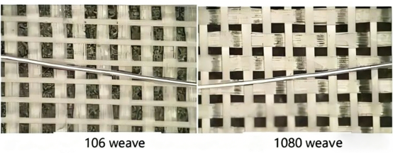
What Is the Fiberglass Effect, and How Do Flattened and Open-Fiber Fabrics Improve High-Speed Signal Performance?
The fiberglass effect refers to signal integrity issues caused by uneven dielectric properties in traditional fiberglass cloth. Flattened fabrics, like 1078 and 1035, and open-fiber processes improve high-speed signal transmission by reducing these inconsistencies.
Why Does Traditional Fiberglass Cloth Cause the "Fiberglass Effect"?
The fiberglass effect arises from gaps between the intersecting fibers in traditional woven cloth, leading to inconsistent dielectric properties and signal delays.
- Warp and Weft Gaps: In conventional fiberglass cloth, the warp (lengthwise) and weft (crosswise) fibers are interwoven, creating tiny gaps or voids at the points where the fibers cross. These gaps result in areas with varying dielectric constants (Dk) across the board.
- Uneven Dielectric Constant: The varying Dk in these gaps means that signals traveling through different sections of the PCB experience different levels of delay, leading to timing mismatches and reduced signal integrity, particularly in high-speed applications.
- Differential Pair Delay Mismatch: In high-speed circuits, especially differential pairs, any delay mismatch can lead to skew and jitter. This can cause errors in the data transmission, affecting the overall performance of the PCB.
Example: In traditional PCBs for consumer electronics, such as motherboards, the fiberglass effect might cause minor signal degradation, but it becomes a significant issue in high-speed applications like 5G or data centers.
How Does the Structure of Flattened Fabrics (e.g., 1078, 1035) Optimize Performance?
Flattened fabrics reduce the gaps between fibers, improving dielectric consistency and reducing signal degradation in high-speed circuits.
- Flattening the Fibers: Flattened fabrics like 1078 and 1035 use a unique manufacturing process where the fibers are pressed or "flattened." This reduces the gaps between the warp and weft threads, creating a more uniform material.
- Reduced Voids: With the reduction of gaps, the dielectric constant becomes more consistent across the board. This leads to fewer variations in signal speed, improving the overall performance of high-speed circuits.
- Improved Dielectric Uniformity: The flattened fibers enhance the dielectric uniformity, which is crucial for maintaining signal integrity, especially at high frequencies.
Example: In advanced mobile devices or high-speed servers, using flattened fabrics ensures that signals travel more evenly across the board, reducing skew and improving performance in high-frequency applications.
How Does the Open-Fiber Process Improve CAF (Conductive Anodic Filament) Reliability?
The open-fiber process disperses the fibers more evenly, increasing surface area and improving resin bonding, which enhances reliability and reduces the risk of conductive anodic filament (CAF) formation.
- Fiber Dispersion: In the open-fiber process, the glass fibers are spread out more evenly compared to traditional weaving methods. This allows for a more even distribution of resin throughout the fiberglass material.
- Increased Surface Area: By dispersing the fibers, the surface area for resin bonding increases, creating a stronger, more stable connection between the resin and the fibers. This enhances the structural integrity of the PCB.
- Reduced CAF Risk: The improved resin bonding reduces the likelihood of CAF, a failure mode where conductive filaments form between PCB layers due to moisture and electrical stress. CAF formation can lead to short circuits and board failures.
Example: In high-reliability industries like aerospace or medical devices, where PCBs need to withstand extreme conditions, using the open-fiber process helps improve durability and long-term performance.
What Is the Significance of Flattened Fabrics in Ultra-Thin PCB Design?
Flattened fabrics allow for thinner PCB designs with more flexible layer configurations, making them ideal for compact and high-performance devices.
- Increased Single Yarn Width: Flattening the fabric increases the width of individual yarns, which reduces the need for densely packed fibers. This helps in achieving thinner boards without sacrificing strength.
- Thinner Boards: Because the fabric density is reduced, the overall thickness of the PCB can be minimized, which is important for applications where space is limited, such as smartphones, wearables, and other compact devices.
- Flexible Layer Configuration: The thinner structure allows for more flexible design options when stacking layers in multilayer PCBs. This increases design versatility and enables the creation of thinner, more complex PCBs.
Example: In mobile phones, using flattened fabrics like 1078 allows for thinner and more flexible PCB designs, which are critical in making devices lighter and more compact without compromising performance.
How to Choose the Right Fiberglass Cloth Type for High-Speed and High-Frequency PCBs?
Selecting the appropriate fiberglass cloth type for high-speed , high-frequency PCBs depends on the signal rate, packaging type, board thickness, and cost-performance balance. Understanding these factors ensures optimal performance and reliability.
How to Choose Fiberglass Cloth Based on Signal Rate?
The choice of fiberglass cloth varies significantly with the required signal speed. Different fiberglass materials are better suited for different data rates.
- <25G Standard Boards: For low to medium-speed PCBs (under 25G), standard fiberglass cloths like E-glass are sufficient. These offer a good balance between cost and performance and are commonly used in consumer electronics or standard multi-layer boards.
- 56G/112G Server Boards: For medium to high-speed applications (e.g., 56G or 112G), NE-glass or L-glass are preferred. These materials provide lower dielectric constants (Dk) and dissipation factors (Df), which help maintain signal integrity and reduce high-frequency losses in servers, data centers, and networking equipment.
- ≥100GHz RF Modules: For ultra-high-speed applications (e.g., 100GHz or more), quartz fabric is the ideal choice due to its extremely low Dk (~2.3) and Df (~0.0009). Quartz minimizes signal delay and loss, making it perfect for RF modules and optical communication systems.
Example: A typical 56G server motherboard will use NE-glass to handle the high-speed signals without significant loss or distortion.
How to Choose Fiberglass Cloth Based on Packaging Type?
The fiberglass cloth selection depends on the packaging form of the components, such as BGA (Ball Grid Array) or FC-BGA (Flip Chip Ball Grid Array), and the specific needs for high-density interconnections.
- BGA (Ball Grid Array): For BGA packages, T-glass is commonly used due to its low coefficient of thermal expansion (CTE), which reduces thermal stress and prevents solder joint failure during temperature cycling.
- FC-BGA Substrates: For FC-BGA packaging, which requires high-density interconnections, T-glass or L-glass is preferred because of their high stiffness, low Dk, and excellent thermal stability
- AI Chip Packaging: In AI processors, which require high power and thermal performance, T-glass is commonly chosen because of its ultra-low CTE, providing thermal expansion matching with the silicon chip, reducing the risk of failure at the solder joints.
Example: AI accelerators like NVIDIA GPUs are typically packaged with T-glass for its thermal stability and precise CTE matching, which helps improve the longevity and reliability of the chip.
How to Choose Fiberglass Cloth Based on Board Thickness and Layer Stack-Up Design?
The fiberglass cloth should be selected based on the desired board thickness, layer stack-up, and the type of PCB design (e.g., HDI, IC substrates).
- Thick Boards: For thicker boards, such as those used in power supplies and traditional multi-layer designs, E-glass or NE-glass is a suitable choice. These materials provide the right balance of mechanical strength and cost-effectiveness for thicker, high-density boards.
- HDI (High-Density Interconnect): For HDI boards, which require precise signal routing in thinner, more compact designs, 1080 (thin cloth) or 2116 fiberglass is ideal. These types offer the necessary flexibility and strength for complex, high-performance designs.
- IC Substrates: For IC substrates (used in semiconductors), T-glass is typically used due to its low Dk, low Df, and low CTE. It ensures minimal signal loss and maximum reliability in high-density, high-performance IC packaging.
Example: For an HDI PCB used in a smartphone, 2116 fiberglass offers the necessary thickness and flexibility for the high-density routing of fine traces.
How to Balance Cost and Performance in Fiberglass Cloth Selection?
The choice of fiberglass cloth should strike a balance between cost and performance, especially when designing for consumer electronics, data centers, or communication devices.
- Consumer Electronics: In consumer-grade PCBs, E-glass is typically chosen due to its cost-effectiveness, providing the necessary mechanical strength for devices like smartphones, laptops, and televisions without the need for premium materials. Although it has a higher Dk and Df, these are acceptable for lower-speed applications.
- Data Centers: For data center applications, NE-glass or L-glass is preferred, as these materials offer lower Dk and Df, ensuring minimal signal loss at high speeds. While more expensive than E-glass, they provide better performance for servers and networking equipment.
- Communication Devices: Communication equipment like routers, switches, and 5G base stations benefit from materials like T-glass or L-glass, which offer low CTE and low signal loss, ensuring high-speed data integrity in high-frequency environments. However, the higher material cost must be justified by the performance needs.
Example: A standard laptop motherboard may use E-glass for cost savings, while a high-performance data center server board may opt for L-glass to ensure minimal signal degradation over long distances and at high frequencies.
Choosing the right fiberglass cloth for high-speed, high-frequency PCBs depends on several factors, including signal rate, packaging type, board thickness, and cost-performance requirements. For higher data rates (56G and above), advanced materials like NE-glass, L-glass, and T-glass provide better performance, while E-glass remains suitable for more cost-sensitive, low-speed applications. Balancing performance with cost ensures that the material selection aligns with the specific needs of different industries, such as consumer electronics, data centers, and communication equipment.
Conclusion
Selecting the right fiberglass cloth for high-speed, high-frequency PCBs is essential for achieving optimal signal integrity, performance, and reliability. With the right choice, whether for consumer electronics, data centers, or high-performance communication devices, you can ensure that your designs meet the demands of modern technology. Understanding the differences between materials like E-glass, NE-glass, and T-glass allows you to balance performance and cost effectively.
For those looking for a trusted partner to deliver high-quality PCBs, PCBMASTER is a seasoned supplier with years of experience in providing custom PCB solutions. Our expertise ensures that you receive precise and reliable products designed for your specific needs, no matter how complex your project may be. Let us help you elevate your designs with the best materials and cutting-edge manufacturing capabilities. Reach out to PCBMASTER today to get started on your next project!
FAQs
Does a Smaller Fiberglass Cloth Model Number Always Mean Better Performance?
No, it does not. The model number primarily represents the thickness specification of the fiberglass cloth, not directly its dielectric properties or material quality. For example, a model like 7628 indicates a thicker cloth used for standard multi-layer PCBs, while a model like 1080 represents a thinner cloth, often used for HDI boards. The dielectric performance (Dk, Df) and material grade are influenced by the specific type of glass used (e.g., E-glass, L-glass, T-glass) rather than the model number alone.
Is Quartz Fabric Necessary for High-Speed PCBs?
Not necessarily. While quartz fabric is excellent for ultra-high-frequency applications (like RF modules with frequencies exceeding 100GHz), most high-speed applications, such as 56G/112G server boards, are well-served by NE-glass or L-glass fabrics. These materials offer lower dielectric constants (Dk) and dissipation factors (Df) suitable for high-speed digital signals, making them more cost-effective for many high-speed applications without sacrificing performance.
Does the Fiberglass Effect Affect All PCBs?
The fiberglass effect is most noticeable in high-speed differential signals, such as those used in PCIe or SerDes (serial-deserialization) interfaces. These high-speed signals are highly sensitive to variations in the dielectric properties of the PCB material, leading to signal delays and integrity issues. However, in low-speed circuits, such as simple power or analog circuits, the fiberglass effect has much less impact and may not cause significant issues.
Can T-glass and Quartz Fabric Be Used Interchangeably?
No, T-glass and quartz fabric cannot fully replace each other. Quartz fabric is mainly chosen for its extremely low dielectric loss (Df), which is ideal for applications requiring minimal signal attenuation, such as in RF modules and optical communications. On the other hand, T-glass excels in applications requiring low CTE (coefficient of thermal expansion) and high modulus, making it suitable for packaging high-performance components like AI chips and FC-BGA substrates, where thermal reliability and mechanical stability are critical. While both materials are excellent for high-performance PCBs, their specific properties make them suited for different types of applications.
Does Using Ultra-Thin Fiberglass Cloth Increase Manufacturing Difficulty?
Yes, using ultra-thin fiberglass cloth increases manufacturing complexity. Thinner fabrics, such as 106/1035, require more precise resin flow control and tighter lamination windows during the manufacturing process. This results in a narrower range of process parameters within which the PCB can be successfully manufactured. Additionally, because the material is thinner, it often requires more careful handling to ensure uniform resin impregnation and prevent defects. As a result, the manufacturing cost increases due to the added complexity in controlling these factors, making it more challenging and expensive to produce ultra-thin PCBs.
Author Bio
Hi, I'm Carol, the Overseas Marketing Manager at PCBMASTER, where I focus on expanding international markets and researching PCB and PCBA solutions. Since 2020, I've been deeply involved in helping our company collaborate with global clients, addressing their technical and production needs in the PCB and PCBA sectors. Over these years, I've gained extensive experience and developed a deeper understanding of industry trends, challenges, and technological innovations.
Outside of work, I'm passionate about writing and enjoy sharing industry insights, market developments, and practical tips through my blog. I hope my posts can help you better understand the PCB and PCBA industries and maybe even offer some valuable takeaways. Of course, if you have any thoughts or questions, feel free to leave a comment below—I'd love to hear from you and discuss further!
About the Author

Carol Luo
PCB Design EngineerI'm Carol, a PCB Engineer at PCBMASTER with experience in PCB design and manufacturing engineering since 2018. I focus on translating engineering requirements into reliable PCB solutions, with expertise in stack-up design, material selection, and design-for-manufacturing (DFM). I share practical engineering insights from real-world PCB design and production experience.
Visit Carol Luo's Profile
